Description
FSM 128NT, FSM 128L Film Stress & Wafer Bow Measurement System – Semiconductor Wafer Metrology
Global film stress measurements at room Temperature
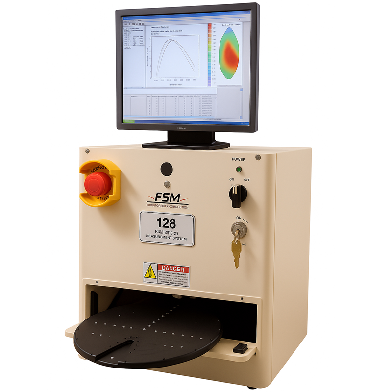
The FSM 128NT and FSM 128L Film Stress & Wafer Bow Measurement Systems are designed for non-contact measurement of semiconductor wafer curvature, wafer bow, and thin film stress characterization. These systems use laser scanning technology and 2D/3D mapping software for semiconductor manufacturing, compound semiconductor applications, MEMS fabrication, thin film deposition, and research laboratories.
The FSM 128 series supports wafer sizes from 50 mm to 300 mm, depending on the model. Dual-laser measurement technology, motorized wafer rotation, and advanced mapping software enable detailed evaluation of wafer deformation, curvature, and calculated film stress.
Key Features and Benefits
- Non-Contact Measurement: Laser scanning technology measures wafer curvature and bow without mechanical contact with the wafer surface.
- Wafer Size Capability: FSM 128NT supports 50–200 mm wafers; FSM 128L supports 50–300 mm wafers.
- Thin Film Stress Measurement: Calculates tensile and compressive film stress using wafer curvature changes and film/substrate properties.
- 2D/3D Mapping: Programmable multiple diametric scans provide detailed wafer bow and curvature maps.
- Dual-Laser Technology: Automatic laser switching accommodates different wafer surfaces and film reflectivities.
- High Measurement Sensitivity: Detects wafer bow height changes as small as 1 micron under specified conditions.
- Motorized Wafer Rotation: Supports measurements at multiple wafer orientations.
- Data Analysis: Software provides wafer curvature, radius of curvature, bow, and calculated film stress results.
- Data Export: Measurement results, tables, graphs, and maps can be exported to Excel-compatible formats and JPEG images.
- Room Temperature Operation: Designed for ambient-temperature wafer metrology.
FSM 128NT and FSM 128L Technical Specifications
| Parameter | Specification |
|---|---|
| Measurement Technology | Non-contact laser scanning |
| Measurement Parameters | Wafer bow, curvature, radius of curvature, thin film stress |
| FSM 128NT Wafer Size | 50–200 mm |
| FSM 128L Wafer Size | 50–300 mm |
| Wafer Thickness | Less than 5 mm |
| Film Stress Range | 1 MPa to 1.4 GPa for specified silicon wafer conditions |
| Bow Sensitivity | 1 micron bow height change under specified conditions |
| Maximum Bow Measurement | Up to 2000 microns |
| Scan Edge Exclusion | 3 mm |
| Mapping Capability | Up to 32 scan lines; 6 recommended |
| Data Acquisition | 40 data points/mm |
| Repeatability | 1% (1 sigma), measured using a 20 m curvature mirror standard |
| Accuracy | Better than 2.5% using a 20 m radius curvature mirror |
| Laser Classification | Class 1 |
| Operating Temperature | Ambient |
| Software Compatibility | Windows 7–11 |
| Data Export | Excel-compatible data and JPEG images |
| Power Requirements | 110V/220V, 20A |
Note: Measurement accuracy, repeatability, and stress sensitivity depend on substrate material, wafer thickness, film properties, and measurement conditions.
FSM 128 Models and Wafer Size Configurations
| Model | Wafer Size | Configuration |
|---|---|---|
| FSM 128NT | 50–200 mm | Semi-automated wafer stress and bow measurement |
| FSM 128L | 50–300 mm | Large-wafer semi-automated stress and bow measurement |
| FSM 128C2C | 150–200 mm | Fully automated cassette-to-cassette measurement |
| FSM 128L C2C | Up to 300 mm | Automated wafer handling with open cassette or FOUP configurations |
Working Principle – Wafer Bow and Film Stress Measurement
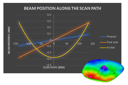
The FSM 128 uses non-contact laser scanning technology to measure semiconductor wafer curvature. A laser beam scans across the wafer surface, and the reflected beam is detected to determine changes in wafer surface slope and curvature.
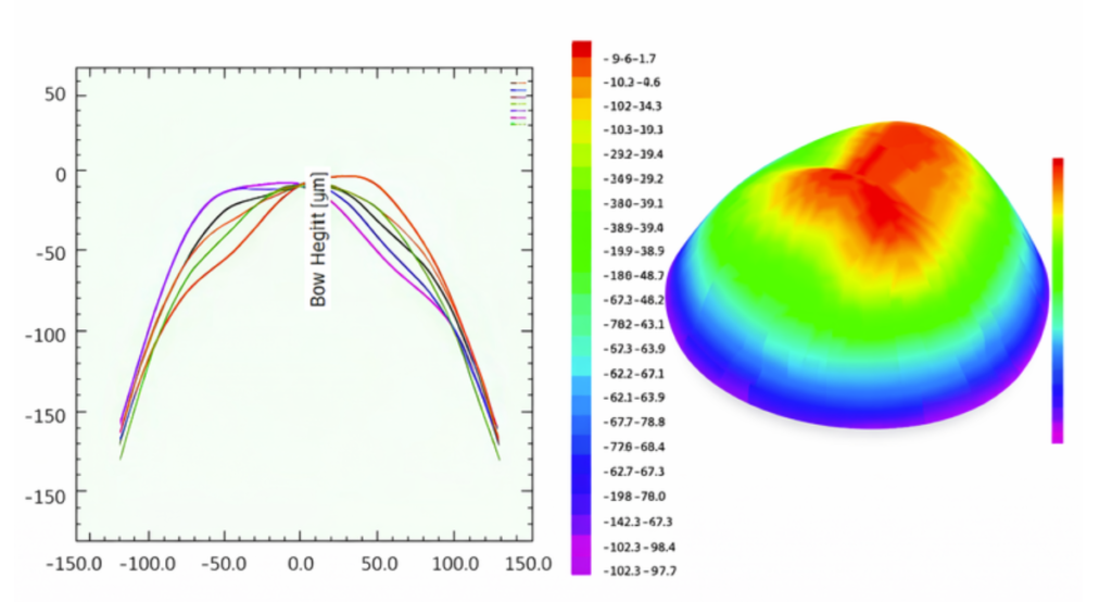
A single scan provides a wafer curvature profile along one direction. Multiple scans at different wafer orientations generate 2D/3D wafer bow and curvature maps.
Thin film stress is calculated from the change in substrate curvature before and after film deposition using the appropriate substrate properties, film thickness, and stress calculation model, such as Stoney’s equation where applicable.
This measurement method enables evaluation of tensile and compressive stress introduced by semiconductor thin film deposition and other manufacturing processes.
Semiconductor and Thin Film Applications
Semiconductor Wafer Manufacturing
- Wafer bow and curvature measurement
- Thin film stress characterization
- Wafer deformation monitoring
- Deposition process development
- Process monitoring and quality control
Compound Semiconductor Applications
The FSM 128 measurement technology is relevant to compound semiconductor wafer characterization, including:
- GaAs semiconductor wafers
- InP semiconductor wafers
- GaN epitaxial structures
- SiC semiconductor substrates
- Compound semiconductor thin film and epitaxial process development
Measurement suitability depends on substrate dimensions, optical reflectivity, material properties, and the selected system configuration.
MEMS and Advanced Semiconductor Devices
- MEMS thin film stress characterization
- Residual stress measurement
- Dielectric and metal film stress evaluation
- Wafer bow monitoring during process development
- Advanced packaging and wafer deformation studies
Thin Film Deposition Processes
The FSM 128 can be used to evaluate wafer curvature changes associated with:
- Physical Vapor Deposition (PVD)
- Chemical Vapor Deposition (CVD)
- Plasma Enhanced Chemical Vapor Deposition (PECVD)
- Atomic Layer Deposition (ALD)
- Epitaxial thin film growth
- Metal and dielectric thin film processing
2D/3D Wafer Bow and Stress Mapping
The FSM 128 supports programmable multiple diametric scans using a motorized wafer rotation stage. Measurements at different wafer orientations allow users to evaluate wafer curvature variations and non-uniform deformation.
The mapping software provides measurement data for process development, film stress characterization, and wafer quality evaluation.
- Single-line wafer curvature measurement
- Multiple-angle wafer scanning
- 2D wafer bow mapping
- 3D wafer surface profiling
- Film stress analysis
- Measurement data export and reporting
System Dimensions and Facilities Requirements
| Parameter | FSM 128NT | FSM 128L |
|---|---|---|
| Width | 14 inches | 14 inches |
| Depth | 20 inches | 28 inches |
| Height | 16 inches | 16 inches |
| Weight | 55 lbs | 60 lbs |
| Electrical Power | 110V/220V, 20A | 110V/220V, 20A |
Computer and Software Requirements
- Intel Core i5 processor or later
- Minimum 2 GB RAM
- 1 TB hard drive
- Four USB ports
- Two Ethernet ports
- Windows-compatible measurement software
FSM 128NT and FSM 128L Equipment Inquiry and Quotation
SemiStar Corp. welcomes inquiries from semiconductor manufacturers, compound semiconductor fabs, MEMS manufacturers, universities, research institutes, and semiconductor process development laboratories.
For an FSM 128NT or FSM 128L equipment inquiry, please provide the required model, wafer size, substrate material, measurement applications, and any special system configuration requirements.
Equipment availability, configuration, pricing, delivery schedule, and commercial terms are subject to confirmation.
Frontier Semiconductor Measurements (FSM) – Semiconductor Metrology Equipment
SemiStar Corp. is a distributor of Frontier Semiconductor Measurements (FSM) semiconductor metrology equipment, providing measurement solutions for semiconductor manufacturing, compound semiconductor fabs, MEMS, advanced packaging, universities, and research laboratories.
FSM specializes in semiconductor wafer metrology and electrical characterization, including thin film stress, wafer bow, wafer curvature, wafer thickness, Total Thickness Variation (TTV), sheet resistance, four-point probe (4PP), and thin film adhesion testing. FSM measurement systems are available in desktop, semi-automatic, and fully automatic cassette-to-cassette configurations, depending on the equipment model.
FSM Semiconductor Metrology Equipment Models
- FSM 128NT / FSM 128L: Thin film stress, wafer bow, and wafer curvature measurement systems.
- FSM 128 C2C / FSM 128L C2C: Automated cassette-to-cassette thin film stress, wafer bow, and curvature measurement systems.
- FSM 500TC: High-temperature thin film stress and wafer curvature measurement system.
- FSM 900TC / FSM 900TC-VAC: High-temperature wafer stress and curvature measurement systems, including vacuum configurations.
- FSM 900TC C2C / FSM 900TC-VAC C2C: Fully automated cassette-to-cassette high-temperature stress and curvature measurement systems.
- FSM 413 MOT: Desktop wafer and thin film thickness measurement system using Echoprobe™ infrared interferometry.
- FSM 413 SA: Semi-automatic wafer and thin film thickness measurement system with enclosure.
- FSM 413 C2C: Fully automatic cassette-to-cassette wafer thickness, thin film thickness, and TTV measurement system.
- FSM 4PP: Contact four-point probe and non-contact sheet resistance measurement systems, including tabletop and automated cassette-to-cassette configurations.
- FSM MELT: Modified Edge Liftoff Test system for thin film and film stack adhesion measurement.
- FSM Aquaflex: Four-point bend film adhesion testing system for low-to-medium adhesion samples.
Semiconductor Metrology Applications
FSM equipment supports semiconductor process development, wafer characterization, thin film deposition evaluation, ion implantation, diffusion, metallization, wafer thinning, wafer bonding, MEMS fabrication, and advanced semiconductor manufacturing.
Contact SemiStar Corp. for FSM semiconductor metrology equipment selection, technical specifications, system configurations, and quotations.