
Description
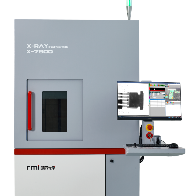
Universal X-RAY X-7900 Inspection System
The X-7900 X-ray Inspection System is a high-performance X-ray inspection solution designed for universities, research institutes, compound semiconductor laboratories, and advanced electronics inspection applications. Compared with entry-level systems, the X-7900 provides higher penetration capability, improved resolution, and stronger inspection performance for semiconductor and advanced material analysis.
Key Features
- 130 kV X-ray inspection system for advanced research and semiconductor applications
- Hamamatsu X-ray tube and Iray Technology flat panel detector
- Higher resolution capability compared with entry-level systems
- 540 × 540 mm stage platform suitable for various sample types
- Strong fit for semiconductor inspection, failure analysis, and advanced material research
Strong Selling Points
- Advanced Research X-ray Inspection Solution
The X-7900 is mainly recommended for universities, research institutes, and compound semiconductor laboratories requiring stronger inspection capability and higher image resolution. - Higher Resolution Capability
With 3–5 μm inspection capability, the X-7900 is suitable for semiconductor device inspection, advanced packaging analysis, and material defect evaluation. - Premium Core Components
The system uses a Hamamatsu X-ray tube and Iray Technology flat panel detector to provide stable image quality and dependable operation. - Strong Fit for Compound Semiconductor Applications
The X-7900 is suitable for GaN, SiC, InP, GaAs, and other compound semiconductor inspection applications requiring better image detail and stronger penetration capability. - Balanced Performance and Cost
The X-7900 provides a strong balance between performance, inspection capability, and investment cost for advanced research and semiconductor users.
Applications
- Compound semiconductor inspection: SiC, GaN, InP, GaAs
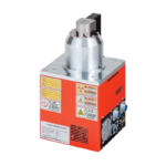
X-ray tube
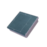
Detector
- BGA and advanced semiconductor packaging inspection
- PCB and electronic component inspection
- Failure analysis and defect review
- Advanced material and research sample evaluation
- University and laboratory X-ray inspection applications
Positioning
The X-7900 is the mid-to-high level model in SemiStar’s X-ray inspection lineup and is mainly recommended for universities, research institutes, compound semiconductor labs, and advanced research users requiring higher resolution and stronger penetration capability than entry-level inspection systems.
Specifications
| Category | Item | Specification |
| X-ray Source | Model | X-7900 |
| Tube Type | Enclosed type | |
| Tube Voltage | 130 kV | |
| Tube Current | 300 μA | |
| Imaging | Spatial Resolution | 3–5 μm |
| Optical / System Magnification | 400X / 1600X | |
| Detector Resolution | 1536 × 1536 pixels | |
| A/D Density Value | 16 bit (65536) | |
| Frame Frequency | 20 FPS | |
| Image Taking Type | Flat-panel digital | |
| Stage / Inspection | Stage Size | 540 × 540 mm |
| Detection Range | 510 × 510 mm | |
| Load-bearing | ≤10 kg | |
| Detector Rotation Angle | 70° | |
| Stage Movement | Automatic / manual | |
| System | Operating System | Windows 11 |
| Power Supply | AC110–220V, 50–60Hz | |
| Power | 1200W | |
| Radiation Safety Test | <1 μSv/h | |
| Machine Size | 1102 × 1360 × 1802 mm (L × W × H) | |
| Machine Size Including Monitor | 1607 × 1903 × 2157 mm (L × W × H) | |
| Machine Weight | 1050 kg |
* Specifications are for reference only and may vary depending on configuration. Please contact SemiStar or the manufacturer for official specifications.
See how the X-7900 compares with other models in resolution, penetration capability, and application range.
View full comparison →