Description
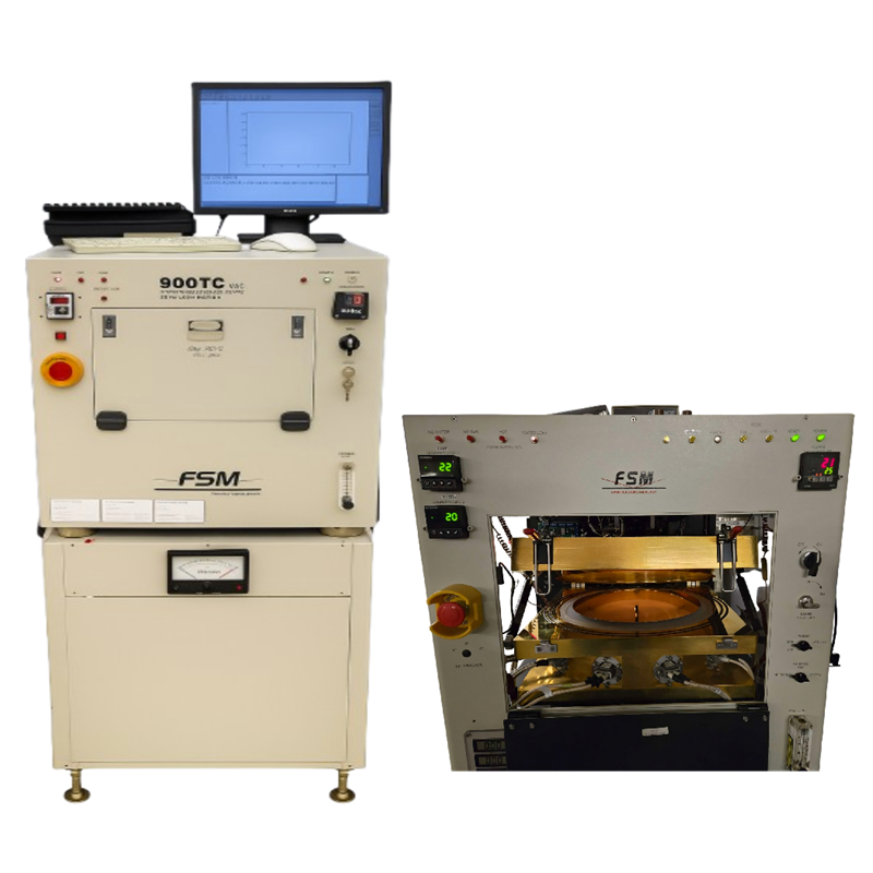
FSM 900TC, FSM 900TC-VAC High-Temperature Film Stress & Wafer Bow Measurement Systems
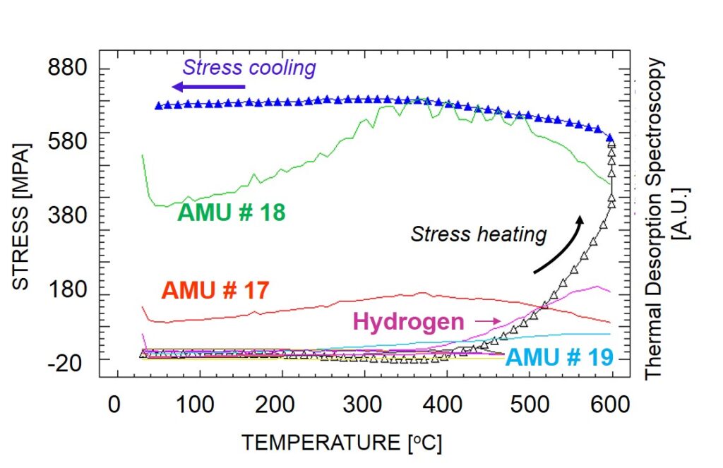
Stress Hysteresis in vacuum or gas up to 900C for the study of annealing cycles. Thermal Desorption, Film Shrinkage, Reflectivity, and Resistivity options provide additional insight to causes of material changes with temperature.
The FSM 900TC and FSM 900TC-VAC High-Temperature Film Stress & Wafer Bow Measurement Systems are designed for non-contact measurement of semiconductor wafer curvature, wafer bow, and thin film stress during programmable thermal cycles. These systems support high-temperature semiconductor material characterization, thin film thermal stress analysis, MEMS fabrication, compound semiconductor applications, and semiconductor process development.
The FSM 900TC provides high-temperature wafer stress measurement, while the FSM 900TC-VAC incorporates a vacuum chamber for thermal characterization under vacuum or controlled gas environments. The FSM 900TC series supports temperature-dependent stress analysis up to 900°C, with an optional 1100°C configuration available for the FSM 900TC-VAC.
Key Features and Benefits
- High-Temperature Measurement: Non-contact wafer curvature, bow, and calculated thin film stress measurement during programmable thermal cycles.
- Temperature Capability: High-temperature characterization up to 900°C, with optional 1100°C capability for the FSM 900TC-VAC.
- Wafer Size Capability: Supports 50–200 mm or 300 mm wafers, depending on model and configuration.
- Non-Contact Measurement: Laser measurement technology evaluates wafer curvature without mechanical contact with the wafer surface.
- Thin Film Stress Measurement: Calculates tensile and compressive film stress using wafer curvature changes and film/substrate properties.
- Programmable Thermal Cycling: Supports temperature ramp, hold, and cooling sequences.
- Temperature Ramp Rate: Programmable heating rates of 1–50°C/min for the published FSM 900TC-VAC configuration.
- Vacuum Measurement: FSM 900TC-VAC supports high-vacuum thermal characterization.
- Controlled Gas Environment: Supports nitrogen, argon, or forming gas, depending on configuration.
- Stress Hysteresis Analysis: Evaluates stress changes during heating and cooling.
- CTE Analysis: Supports coefficient of thermal expansion calculations.
- Integrated Metrology: FSM 900TC-VAC supports thermal desorption analysis and optional additional metrology capabilities.
- Optional 2D/3D Mapping: Wafer curvature and stress mapping capability, depending on configuration.
- Data Analysis and Reporting: Measurement software supports stress versus temperature, stress versus time, and wafer bow analysis.
FSM 900TC and FSM 900TC-VAC Models and Configurations
| Model | Configuration | Primary Applications |
|---|---|---|
| FSM 900TC | High-temperature wafer stress and bow measurement system | Thermal stress, wafer curvature, thin film characterization, and process development |
| FSM 900TC-VAC | High-temperature vacuum wafer stress and bow measurement system | Vacuum thermal cycling, stress hysteresis, thermal desorption, and advanced thin film characterization |
FSM 900TC and FSM 900TC-VAC Technical Specifications
| Parameter | FSM 900TC | FSM 900TC-VAC |
|---|---|---|
| Equipment Type | High-temperature film stress measurement | High-temperature vacuum film stress measurement |
| Measurement Technology | Non-contact laser measurement | Non-contact laser triangulation |
| Measurement Parameters | Wafer bow, curvature, calculated film stress | Wafer bow, curvature, calculated film stress, stress hysteresis |
| Wafer Size | Configuration dependent | 50–200 mm / 300 mm, depending on configuration |
| Standard Maximum Temperature | 900°C | 900°C |
| Optional Maximum Temperature | Subject to confirmation | 1100°C |
| Temperature Ramp Rate | Configuration dependent | 1–50°C/min, programmable |
| Thermal Cycling | Programmable ramp and hold | Programmable ramp and hold |
| Heating Method | Configuration dependent | Tungsten halogen lamps |
| Vacuum Capability | Not specified | Down to 5 × 10⁻⁶ Torr |
| Vacuum Pumping | Not specified | Turbomolecular pump with dry pump |
| Process Gas | Configuration dependent | Nitrogen, argon, forming gas |
| Thermal Desorption Analysis | Not specified | Integrated TDS capability |
| Film Thickness Measurement | Not specified | Optional |
| Reflectivity Measurement | Not specified | Optional |
| Sheet Resistance Measurement | Not specified | Optional |
| 2D/3D Stress Mapping | Configuration dependent | Optional |
| Electrical Power | Subject to confirmation | 208 V, 30 A, 3-phase, 5-wire |
Note: The published technical specifications are primarily for the FSM 900TC-VAC. FSM 900TC specifications and optional configurations require confirmation. Measurement performance depends on substrate material, wafer thickness, film properties, and measurement conditions.
Working Principle – High-Temperature Wafer Bow and Film Stress Measurement
The FSM 900TC and FSM 900TC-VAC use non-contact laser measurement technology to evaluate semiconductor wafer curvature during programmable thermal cycles.
As the wafer is heated, changes in substrate curvature are measured and analyzed to determine temperature-dependent deformation and thin film stress behavior.
Thin film stress is calculated using wafer curvature measurements, substrate mechanical properties, film thickness, and an appropriate stress calculation model, such as Stoney’s equation where applicable.
The FSM 900TC-VAC incorporates a vacuum heating chamber with tungsten halogen lamps and reflective chamber walls. This configuration supports thermal characterization under vacuum or controlled gas environments.
By measuring wafer curvature during heating, temperature holding, and cooling, the systems support analysis of thermal stress, residual stress, stress relaxation, and hysteresis.
High-Temperature Thermal Cycling and Stress Characterization
The FSM 900TC series is designed for evaluating thin film stress and wafer deformation during high-temperature processing.
The published FSM 900TC-VAC configuration supports programmable heating rates from 1–50°C/min and temperature measurement cycles up to 900°C, with an optional 1100°C configuration.
- Room-temperature wafer curvature measurement
- Programmable high-temperature heating cycles
- Temperature ramp and hold programs
- Stress versus temperature analysis
- Stress versus time analysis
- Wafer bow versus temperature analysis
- Residual stress characterization
- Stress relaxation during temperature holding
- Heating and cooling hysteresis evaluation
- Coefficient of thermal expansion analysis
- Thin film thermal stability studies
FSM 900TC-VAC Vacuum and Inert Gas Thermal Measurement
The FSM 900TC-VAC provides a vacuum measurement environment for characterizing semiconductor materials that are sensitive to oxidation and atmospheric exposure during heating.
The system uses a turbomolecular pumping system with a dry pump and supports vacuum levels down to 5 × 10⁻⁶ Torr under specified conditions.
In addition to vacuum operation, the chamber supports nitrogen, argon, and forming gas environments.
These capabilities are particularly relevant to low-k dielectric materials, copper metallization, advanced thin films, and other materials requiring controlled thermal environments.
- High-vacuum thermal characterization
- Inert gas thermal cycling
- Oxidation-sensitive thin film evaluation
- Low-k dielectric material characterization
- Copper metallization thermal stability studies
- Thin film outgassing analysis
- Vacuum annealing process simulation
FSM 900TC-VAC Integrated Metrology Capabilities
The FSM 900TC-VAC combines high-temperature wafer stress measurement with a vacuum heating chamber and integrated metrology capabilities.
Depending on the selected configuration, the system supports thermal desorption analysis and additional thin film characterization measurements.
| Measurement Capability | Configuration | Application |
|---|---|---|
| Film Stress Measurement | Standard | Wafer curvature, bow, and thermal stress characterization |
| Vacuum Heating Chamber | Standard | Thermal characterization under vacuum or inert gas |
| Thermal Desorption Spectroscopy | Integrated capability | Outgassing and thermal desorption analysis |
| Film Thickness Measurement | Optional | Film thickness and shrinkage measurement |
| Reflectivity Measurement | Optional | Optical reflectivity characterization |
| Sheet Resistance Measurement | Optional | Electrical thin film characterization |
| 2D/3D Stress Mapping | Optional | Wafer curvature and stress distribution analysis |
| 1100°C Temperature Capability | Optional | Extended high-temperature material characterization |
Semiconductor and Thin Film Applications
Semiconductor Wafer Manufacturing
- High-temperature wafer bow and curvature measurement
- Temperature-dependent thin film stress characterization
- Wafer deformation monitoring during thermal cycling
- Thin film thermal stability evaluation
- Annealing process development
- Semiconductor process monitoring and quality control
Compound Semiconductor Applications
The FSM 900TC and FSM 900TC-VAC measurement technology is relevant to compound semiconductor wafer characterization, including:
- GaAs semiconductor wafers
- InP semiconductor wafers
- GaN epitaxial structures
- SiC semiconductor substrates
- III-V semiconductor thin films
- Compound semiconductor epitaxial process development
- Temperature-dependent wafer curvature and stress characterization
Measurement suitability depends on substrate dimensions, optical reflectivity, material properties, thermal stability, and the selected system configuration.
MEMS and Advanced Semiconductor Devices
- MEMS thin film thermal stress characterization
- Residual stress and stress relaxation measurement
- Dielectric and metal film thermal stability evaluation
- Wafer bow monitoring during thermal cycling
- Advanced packaging material characterization
- Thermal mismatch and deformation studies
Thin Film Deposition Processes
The systems can be used to evaluate temperature-dependent wafer curvature and film stress associated with:
- Physical Vapor Deposition (PVD)
- Chemical Vapor Deposition (CVD)
- Plasma Enhanced Chemical Vapor Deposition (PECVD)
- Atomic Layer Deposition (ALD)
- Epitaxial thin film growth
- Metal and dielectric thin film processing
- Thin film annealing and thermal treatment
Advanced Materials and Device Applications
- Low-k dielectric materials
- Copper and advanced metallization films
- Semiconductor interconnect materials
- Solar cell materials
- LED and optoelectronic materials
- Advanced semiconductor packaging materials
Thermal Stress, Stress Relaxation and CTE Analysis
The FSM 900TC and FSM 900TC-VAC provide temperature-dependent wafer curvature and film stress data for evaluating material behavior during thermal processing.
Thermal cycling measurements can help identify stress changes associated with material expansion, contraction, structural relaxation, and temperature-dependent film properties.
The systems support coefficient of thermal expansion (CTE) analysis and evaluation of thermal mismatch between thin films and semiconductor substrates.
- Stress versus temperature analysis
- Stress versus time analysis
- Wafer bow versus temperature analysis
- Residual stress characterization
- Stress relaxation during temperature holding
- Heating and cooling hysteresis evaluation
- Coefficient of thermal expansion calculations
- Thin film thermal stability studies
Thin Film Reliability and Thermal Stability Evaluation
High-temperature wafer stress and curvature measurements are important for understanding the reliability of semiconductor thin films subjected to thermal processing.
The FSM 900TC and FSM 900TC-VAC help researchers and process engineers evaluate stress-related material behavior during heating and cooling.
Temperature-dependent measurements can support material selection, process optimization, and evaluation of potential reliability concerns associated with thermal expansion mismatch, film cracking, delamination, and structural changes.
- Thermal stress accumulation
- Residual stress characterization
- Stress relaxation and hysteresis
- Thin film cracking risk evaluation
- Film and substrate thermal mismatch
- Material thermal stability
- Process temperature optimization
FSM 900TC-VAC System Dimensions and Facilities Requirements
The following specifications apply to the published FSM 900TC-VAC configuration. FSM 900TC facilities and dimensions require separate confirmation.
| Parameter | FSM 900TC-VAC |
|---|---|
| Main Unit Width | 26 inches |
| Main Unit Depth | 58.24 inches |
| Accessory Cart Width | 20 inches |
| Accessory Cart Depth | 20 inches |
| Published Weight | 400 lbs |
| Electrical Power | 208 V, 30 A, 3-phase, 5-wire |
| Cooling Method | Water cooling |
| Vacuum Pumping | Turbomolecular pumping system with dry pump |
| Process Gases | Nitrogen, argon, forming gas |
Note: Equipment dimensions, weight, cooling water requirements, vacuum pumping configuration, and electrical facilities must be confirmed for the selected system.
Computer and Software Capabilities
- Windows-compatible measurement and analysis software
- Programmable temperature ramp and hold recipes
- High-temperature wafer curvature measurement
- Film stress versus temperature analysis
- Film stress versus time analysis
- Wafer bow versus temperature analysis
- Stress hysteresis characterization
- Coefficient of thermal expansion calculations
- Integrated thermal desorption data analysis for FSM 900TC-VAC, depending on configuration
- Optional 2D/3D stress mapping
- Measurement data and graph export
FSM 900TC and FSM 900TC-VAC Equipment Inquiry and Quotation
SemiStar Corp. welcomes inquiries from semiconductor manufacturers, compound semiconductor fabs, MEMS manufacturers, universities, research institutes, and semiconductor process development laboratories.
For an FSM 900TC or FSM 900TC-VAC equipment inquiry, please provide the required model, wafer size, substrate material, film material and thickness, maximum measurement temperature, thermal cycling requirements, vacuum or inert gas requirements, and any special metrology requirements.
Equipment availability, configuration, pricing, delivery schedule, and commercial terms are subject to confirmation.
Frontier Semiconductor Measurements (FSM) – Semiconductor Metrology Equipment
SemiStar Corp. is a distributor of Frontier Semiconductor Measurements (FSM) semiconductor metrology equipment, providing measurement solutions for semiconductor manufacturing, compound semiconductor fabs, MEMS, advanced packaging, universities, and research laboratories.
FSM specializes in semiconductor wafer metrology and electrical characterization, including thin film stress, wafer bow, wafer curvature, wafer thickness, Total Thickness Variation (TTV), sheet resistance, four-point probe (4PP), and thin film adhesion testing. FSM measurement systems are available in desktop, semi-automatic, and fully automatic cassette-to-cassette configurations, depending on the equipment model.
FSM Semiconductor Metrology Equipment Models
- FSM 128NT / FSM 128L: Thin film stress, wafer bow, and wafer curvature measurement systems.
- FSM 128 C2C / FSM 128L C2C: Automated cassette-to-cassette thin film stress, wafer bow, and curvature measurement systems.
- FSM 500TC: High-temperature thin film stress and wafer curvature measurement system.
- FSM 900TC / FSM 900TC-VAC: High-temperature wafer stress and curvature measurement systems, including vacuum configurations.
- FSM 900TC C2C / FSM 900TC-VAC C2C: Fully automated cassette-to-cassette high-temperature stress and curvature measurement systems.
- FSM 413 MOT: Desktop wafer and thin film thickness measurement system using Echoprobe™ infrared interferometry.
- FSM 413 SA: Semi-automatic wafer and thin film thickness measurement system with enclosure.
- FSM 413 C2C: Fully automatic cassette-to-cassette wafer thickness, thin film thickness, and TTV measurement system.
- FSM 4PP: Contact four-point probe and non-contact sheet resistance measurement systems, including tabletop and automated cassette-to-cassette configurations.
- FSM MELT: Modified Edge Liftoff Test system for thin film and film stack adhesion measurement.
- FSM Aquaflex: Four-point bend film adhesion testing system for low-to-medium adhesion samples.
Semiconductor Metrology Applications
FSM equipment supports semiconductor process development, wafer characterization, thin film deposition evaluation, ion implantation, diffusion, metallization, wafer thinning, wafer bonding, MEMS fabrication, and advanced semiconductor manufacturing.
Contact SemiStar Corp. for FSM semiconductor metrology equipment selection, technical specifications, system configurations, and quotations.