Description
FSM 4PP – Four-Point Probe Sheet Resistance Measurement Systems
Electrical Characterization
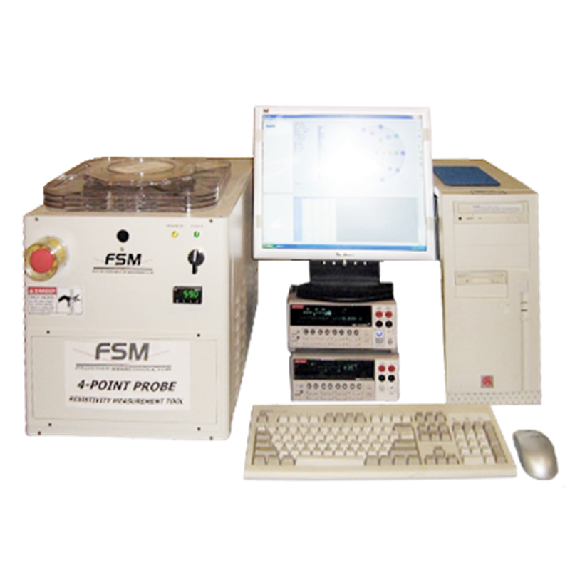
SemiStar Corp. offers FSM 4PP – Four-Point Probe Sheet Resistance Measurement Systems for semiconductor electrical characterization applications.
Contact and non-contact sheet resistance measurement systems are available for implantation, diffusion, metallization, and many other semiconductor applications.
The four-point probe technique is used to measure the sheet resistance of epitaxial layers, metal films, and semiconductor substrates.
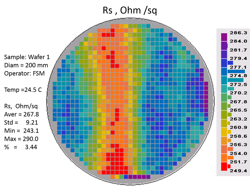
Equipment configurations include tabletop systems and fully automated cassette-to-cassette measurement systems.
Measurement Applications
- Ion implantation
- Diffusion
- Metallization
- Epitaxial layers
- Metal films
- Semiconductor substrates
- Other sheet resistance measurement applications
Available Measurement Systems
| Category | Available Options |
|---|---|
| Measurement Application | Sheet resistance measurement |
| Measurement Methods | Contact and non-contact |
| Measurement Technology | Four-point probe technique for contact sheet resistance measurement |
| Materials and Structures | Epitaxial layers, metal films, semiconductor substrates |
| Equipment Configurations | Tabletop and fully automated cassette-to-cassette systems |
| Semiconductor Processes | Implantation, diffusion, metallization, and other applications |
4PP – Four-Point Probe Sheet Resistance Measurement System Inquiry and Quotation
SemiStar Corp. welcomes inquiries from semiconductor manufacturers, compound semiconductor fabs, MEMS manufacturers, advanced packaging facilities, universities, research institutes, and semiconductor process development laboratories.
For a 4PP – Four-Point Probe Sheet Resistance Measurement System inquiry, please provide the following information:
- Wafer size
- Substrate material
- Minimum and maximum wafer thickness
- Required sheet resistance measurement range
- Contact or non-contact measurement requirements
- Tabletop or fully automated cassette-to-cassette system requirements
Equipment availability, configuration, pricing, delivery schedule, and commercial terms are subject to confirmation.
Frontier Semiconductor Measurements (FSM) – Semiconductor Metrology Equipment
SemiStar Corp. is a distributor of Frontier Semiconductor Measurements (FSM) semiconductor metrology equipment, providing measurement solutions for semiconductor manufacturing, compound semiconductor fabs, MEMS, advanced packaging, universities, and research laboratories.
FSM specializes in semiconductor wafer metrology and electrical characterization, including thin film stress, wafer bow, wafer curvature, wafer thickness, Total Thickness Variation (TTV), sheet resistance, four-point probe (4PP), and thin film adhesion testing. FSM measurement systems are available in desktop, semi-automatic, and fully automatic cassette-to-cassette configurations, depending on the equipment model.
FSM Semiconductor Metrology Equipment Models
- FSM 128NT / FSM 128L: Thin film stress, wafer bow, and wafer curvature measurement systems.
- FSM 128 C2C / FSM 128L C2C: Automated cassette-to-cassette thin film stress, wafer bow, and curvature measurement systems.
- FSM 500TC: High-temperature thin film stress and wafer curvature measurement system.
- FSM 900TC / FSM 900TC-VAC: High-temperature wafer stress and curvature measurement systems, including vacuum configurations.
- FSM 900TC C2C / FSM 900TC-VAC C2C: Fully automated cassette-to-cassette high-temperature stress and curvature measurement systems.
- FSM 413 MOT: Desktop wafer and thin film thickness measurement system using Echoprobe™ infrared interferometry.
- FSM 413 SA: Semi-automatic wafer and thin film thickness measurement system with enclosure.
- FSM 413 C2C: Fully automatic cassette-to-cassette wafer thickness, thin film thickness, and TTV measurement system.
- FSM 4PP: Contact four-point probe and non-contact sheet resistance measurement systems, including tabletop and automated cassette-to-cassette configurations.
- FSM MELT: Modified Edge Liftoff Test system for thin film and film stack adhesion measurement.
- FSM Aquaflex: Four-point bend film adhesion testing system for low-to-medium adhesion samples.
Semiconductor Metrology Applications
FSM equipment supports semiconductor process development, wafer characterization, thin film deposition evaluation, ion implantation, diffusion, metallization, wafer thinning, wafer bonding, MEMS fabrication, and advanced semiconductor manufacturing.
Contact SemiStar Corp. for FSM semiconductor metrology equipment selection, technical specifications, system configurations, and quotations.