Description
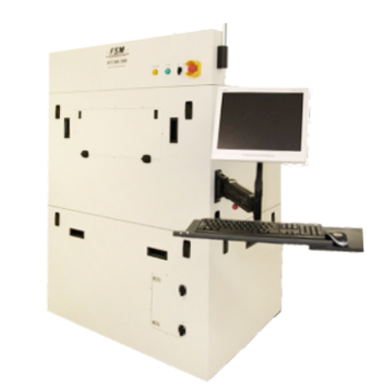
FSM 413 SA Semi-Automatic Wafer and Thin Film Thickness Measurement System with Enclosure
Substrate and tape total and individual thicknesses, warpage, and TTV Measurement. Able to measure with or without backing tape. For wafer back-grind and etch thinning processes control. Non-contact Echoprobe or VITE Technology. Thin film and surface roughness options.
Thickness and total thickness variation (TTV) mapping system. TTV and Thickness of wafer substrate, thick layers, wafers on tape, bonded wafers, etc. Semi-automatic system with enclosure. Manual loading, automatic measurement. Warp, Roughness, and Thin Film Thickness measurement options. Systems up to 300mm diameter wafers with or without frame.
The FSM 413 SA Semi-Automatic Wafer and Thin Film Thickness Measurement System is an enclosed semiconductor metrology platform designed for non-contact wafer thickness measurement, thin film thickness characterization, and Total Thickness Variation (TTV) analysis.
Manufactured by Frontier Semiconductor Measurements (FSM), the FSM 413 SA incorporates patented Echoprobe™ infrared interferometry technology and an automatic X-Y measurement stage. The system provides the same core measurement capabilities as the FSM 413 MOT desktop model, with an enclosed equipment configuration for semiconductor manufacturing, process development, and research applications.
The FSM 413 SA supports compatible silicon, GaAs, InP, SiC, glass, quartz, sapphire, and bonded wafer structures. Available single-probe and dual-probe configurations support semiconductor wafer thickness inspection, ultra-thin wafer measurement, MEMS fabrication, advanced packaging, and substrate characterization.
Key Features and Benefits
- Enclosed Semi-Automatic System: Equipment enclosure with manual wafer loading and automatic measurement operation.
- Non-Contact IR Interferometry: Patented Echoprobe™ technology for semiconductor wafer thickness measurement.
- Automatic X-Y Stage: Programmable measurement locations and wafer thickness mapping.
- Single-Probe Thickness Measurement: Standard measurement range of 15–780 µm.
- Dual-Probe Thickness Measurement: Total thickness measurement up to 3 mm.
- High Measurement Repeatability: 0.2 µm (1σ) for single-probe measurement and 0.7 µm (1σ) for dual-probe measurement.
- Wafer Size: Configurations for wafers up to 150 mm, 200 mm, or 300 mm, with customized sizes available.
- IR Wavelength: 1.3 ± 0.03 µm.
- Total Thickness Variation: TTV measurement and wafer thickness uniformity analysis.
- 2D/3D Thickness Mapping: Color maps for wafer thickness distribution analysis.
- Ultra-Thin Wafer Applications: Supports compatible backgrind and chemically etched wafers.
- Bonded Wafer Measurement: Supports suitable Si/Si, Si/Glass, Si/Tape, and other bonded structures.
- Optional Pattern Recognition: Targeted measurement capability for patterned substrates.
- Optional Advanced Metrology: TSV depth, trench depth, bump height, membrane, and surface roughness measurement functions.
- Compound Semiconductor Applications: Supports compatible GaAs, InP, SiC, and other semiconductor materials.
FSM 413 SA Technical Specifications
| Parameter | Specification |
|---|---|
| Manufacturer | Frontier Semiconductor Measurements (FSM) |
| Equipment Model | FSM 413 SA |
| Equipment Type | Semi-Automatic Wafer and Thin Film Thickness Measurement System |
| System Configuration | Semi-automatic system with enclosure |
| Wafer Loading | Manual wafer loading and unloading |
| Measurement Technology | Non-contact infrared interferometry |
| Sensor Technology | Echoprobe™ IR interferometry sensor |
| Probe Configuration | Single Probe or Dual Probe |
| Wafer Size | Up to 150 mm, 200 mm, or 300 mm; customized sizes available |
| Supported Substrates | Si, GaAs, InP, SiC, Quartz, Glass, Sapphire |
| Single-Probe Thickness Range | 15–780 µm |
| Dual-Probe Total Thickness Range | Up to 3 mm |
| Single-Probe Repeatability | 0.2 µm (1σ) |
| Dual-Probe Repeatability | 0.7 µm (1σ) |
| Display Resolution | 0.1 µm |
| IR Wavelength | 1.3 ± 0.03 µm |
| Thin Film Thickness Option | 1–25 µm |
| Measurement Points | Programmable |
| Wafer Positioning | Automatic X-Y stage |
| High-Precision X-Y Stage | 0.5 µm precision option |
| Measurement Results | TTV, Mean, Maximum, Minimum, Standard Deviation |
| Thickness Mapping | 2D and 3D color maps |
| Pattern Recognition | Optional |
| Surface Roughness Measurement | Optional |
| Bump Height Measurement | Optional |
| Trench and TSV Measurement | Optional |
| Microscope Measurement Option | Available for silicon via depth measurement |
Note: FSM 413 SA shares the FSM 413 MOT core measurement technology and specifications. Available options and performance depend on the selected probe configuration and substrate material. The primary system difference is the enclosed semi-automatic configuration.
FSM 413 SA vs. FSM 413 MOT vs. FSM 413 C2C
| Feature | FSM 413 MOT | FSM 413 SA | FSM 413 C2C |
|---|---|---|---|
| System Type | Desktop | Enclosed Semi-Automatic | Fully Automatic |
| Enclosure | Open desktop configuration | Yes | Yes |
| Wafer Loading | Manual | Manual | Automatic robotic handling |
| Measurement Stage | Automatic X-Y | Automatic X-Y | Automatic X-Y |
| Cassette-to-Cassette | No | No | Yes |
| Measurement Technology | Echoprobe™ IR | Echoprobe™ IR | Echoprobe™ IR |
Working Principle – Echoprobe™ Infrared Interferometry
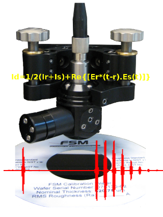
The FSM 413 SA uses patented Echoprobe™ infrared interferometry technology for non-contact semiconductor wafer thickness measurement.
Infrared interferometry detects reflected optical signals from substrate surfaces and material interfaces. For compatible IR-transmitting substrates, thickness is calculated using the optical response and the material’s refractive index.
The optional dual-probe configuration measures total thickness using measurements from opposite sides of the substrate, extending the measurement capability to compatible multilayer and non-transparent structures.
The non-contact measurement method is suitable for semiconductor wafer inspection and thin substrate characterization where mechanical contact with the measurement probe is undesirable.
Enclosed Semi-Automatic System Configuration
The FSM 413 SA incorporates an equipment enclosure around the wafer measurement platform.
Unlike the open desktop FSM 413 MOT configuration, the FSM 413 SA provides an enclosed semi-automatic measurement system while retaining manual wafer loading and unloading.
After the operator loads the wafer, the automatic X-Y stage performs programmable thickness measurements at selected locations across the substrate.
The enclosure provides a defined measurement area for semiconductor wafer metrology. The FSM 413 SA does not require cassette-to-cassette robotic wafer handling.
Single-Probe and Dual-Probe Thickness Measurement
| Feature | Single Probe | Dual Probe |
|---|---|---|
| Thickness Range | 15–780 µm | Up to 3 mm |
| Repeatability | 0.2 µm (1σ) | 0.7 µm (1σ) |
| Primary Application | Substrate thickness and TTV measurement | Total thickness measurement of compatible substrates and wafer stacks |
| Non-Transparent Materials | Limited by IR transmission | Total thickness measurement capability |
Total Thickness Variation (TTV) and Wafer Thickness Mapping
The FSM 413 SA supports programmable measurement locations using its automatic X-Y stage.
Thickness measurements collected across the wafer can be analyzed to evaluate Total Thickness Variation (TTV) and substrate thickness uniformity.
- Total Thickness Variation (TTV)
- Mean wafer thickness
- Maximum thickness
- Minimum thickness
- Standard deviation
- 2D thickness color maps
- 3D thickness color maps
- Programmable measurement points
Ultra-Thin Wafer and Backgrinding Applications
The FSM 413 SA supports semiconductor wafer thickness measurement for backgrinding, chemical etching, and thin wafer manufacturing applications.
- Ultra-thin silicon wafer thickness measurement
- Wafer backgrinding thickness uniformity
- Chemically etched wafer thickness measurement
- Thin wafer substrate characterization
- Wafer thickness mapping
- Backgrinding process development
- Thin wafer process qualification
Specialized thin silicon wafer measurements may require a dedicated measurement configuration. The standard single-probe thickness measurement range is 15–780 µm.
Bonded Wafer and Multilayer Thickness Measurement
The FSM 413 SA supports thickness characterization of compatible bonded wafer structures used in semiconductor manufacturing and advanced packaging.
- Silicon-to-silicon bonded wafers
- Silicon-to-glass bonded wafers
- Silicon wafers mounted on grinding tape
- Silicon wafers mounted on carrier tape
- Compatible multilayer semiconductor substrates
- Advanced packaging wafer stacks
- Wafer bonding uniformity evaluation
The optional dual-probe configuration extends total thickness measurement capability to suitable multilayer and non-transparent structures.
Optional MEMS, TSV and Advanced Metrology Applications
The FSM 413 SA can be configured with additional measurement functions for specialized semiconductor and MEMS applications.
- Trench depth measurement
- Through-silicon via (TSV) depth measurement
- TSV width measurement
- Bump height measurement
- Surface roughness characterization
- MEMS membrane measurement
- Pattern recognition
- Silicon via depth measurement with microscope option
Optional measurement functions require the corresponding hardware and software configuration.
Semiconductor and Compound Semiconductor Applications
Silicon Semiconductor Manufacturing
- Silicon wafer thickness inspection
- Wafer thickness uniformity measurement
- Backgrinding process monitoring
- Wafer thinning process development
- Wafer bonding thickness characterization
- Advanced semiconductor packaging
- MEMS substrate characterization
GaAs and InP Semiconductor Applications
- GaAs wafer thickness measurement
- InP wafer thickness measurement
- Compound semiconductor wafer thinning
- Thin substrate characterization
- RF semiconductor process development
- Photonic semiconductor manufacturing
SiC, Sapphire, Glass and Quartz Applications
- SiC substrate thickness measurement
- Sapphire wafer thickness measurement
- Glass substrate thickness measurement
- Quartz substrate thickness measurement
- Advanced semiconductor material characterization
Computer and Measurement Software
The FSM 413 SA supports programmable measurement locations and wafer thickness data analysis.
- Automatic X-Y stage measurement sequences
- Programmable measurement points
- Wafer thickness measurement
- Total Thickness Variation analysis
- Mean, maximum, and minimum thickness calculations
- Standard deviation analysis
- 2D thickness color maps
- 3D thickness color maps
- Optional pattern recognition
- Optional specialized MEMS measurement functions
FSM 413 SA Wafer Thickness Measurement System Inquiry and Quotation
SemiStar Corp. welcomes inquiries from semiconductor manufacturers, compound semiconductor fabs, MEMS manufacturers, advanced packaging facilities, universities, research institutes, and semiconductor process development laboratories.
For an FSM 413 SA equipment inquiry, please provide the wafer size, substrate material, minimum and maximum wafer thickness, single-probe or dual-probe requirements, bonded wafer or carrier configuration, and any optional measurement requirements such as TTV, TSV depth, trench depth, bump height, or surface roughness.
Equipment availability, configuration, pricing, delivery schedule, and commercial terms are subject to confirmation.
Frontier Semiconductor Measurements (FSM) – Semiconductor Metrology Equipment
SemiStar Corp. is a distributor of Frontier Semiconductor Measurements (FSM) semiconductor metrology equipment, providing measurement solutions for semiconductor manufacturing, compound semiconductor fabs, MEMS, advanced packaging, universities, and research laboratories.
FSM specializes in semiconductor wafer metrology and electrical characterization, including thin film stress, wafer bow, wafer curvature, wafer thickness, Total Thickness Variation (TTV), sheet resistance, four-point probe (4PP), and thin film adhesion testing. FSM measurement systems are available in desktop, semi-automatic, and fully automatic cassette-to-cassette configurations, depending on the equipment model.
FSM Semiconductor Metrology Equipment Models
- FSM 128NT / FSM 128L: Thin film stress, wafer bow, and wafer curvature measurement systems.
- FSM 128 C2C / FSM 128L C2C: Automated cassette-to-cassette thin film stress, wafer bow, and curvature measurement systems.
- FSM 500TC: High-temperature thin film stress and wafer curvature measurement system.
- FSM 900TC / FSM 900TC-VAC: High-temperature wafer stress and curvature measurement systems, including vacuum configurations.
- FSM 900TC C2C / FSM 900TC-VAC C2C: Fully automated cassette-to-cassette high-temperature stress and curvature measurement systems.
- FSM 413 MOT: Desktop wafer and thin film thickness measurement system using Echoprobe™ infrared interferometry.
- FSM 413 SA: Semi-automatic wafer and thin film thickness measurement system with enclosure.
- FSM 413 C2C: Fully automatic cassette-to-cassette wafer thickness, thin film thickness, and TTV measurement system.
- FSM 4PP: Contact four-point probe and non-contact sheet resistance measurement systems, including tabletop and automated cassette-to-cassette configurations.
- FSM MELT: Modified Edge Liftoff Test system for thin film and film stack adhesion measurement.
- FSM Aquaflex: Four-point bend film adhesion testing system for low-to-medium adhesion samples.
Semiconductor Metrology Applications
FSM equipment supports semiconductor process development, wafer characterization, thin film deposition evaluation, ion implantation, diffusion, metallization, wafer thinning, wafer bonding, MEMS fabrication, and advanced semiconductor manufacturing.
Contact SemiStar Corp. for FSM semiconductor metrology equipment selection, technical specifications, system configurations, and quotations.