
Description
X-RAY Inspection Systems Comparison
SemiStar provides X-ray inspection systems for universities, research institutes, compound semiconductor laboratories, and advanced electronics inspection applications. Our X-ray product lineup covers applications from affordable research inspection systems to high-resolution 3D/CT semiconductor analysis platforms.
Product Line: X-7100 | X-7900 | X-9200 | X-7900 ULTRA
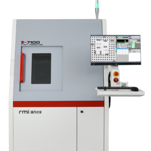
X-7100
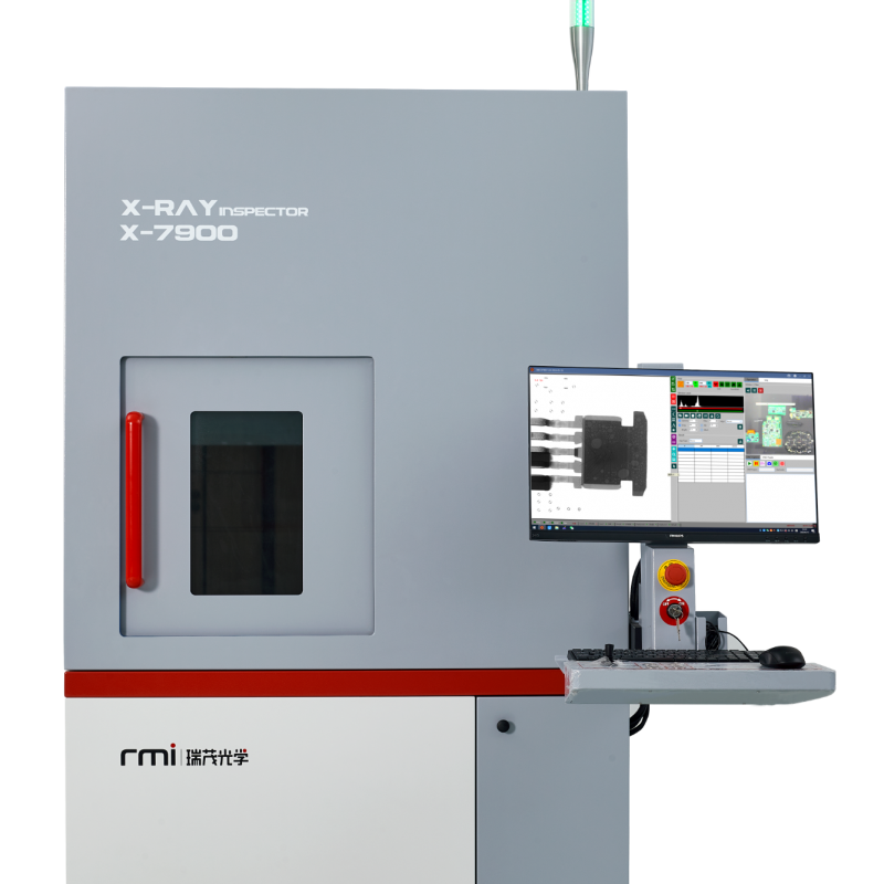
X-7900

X-9200

X-7900 ULTRA

X-RAY Inspection Systems Customers
Model Comparison
| Item | X-7100 | X-7900 | X-9200 | X-7900 ULTRA |
| Positioning | Entry-level research inspection | Advanced research and semiconductor inspection | Large-platform inspection system | High-end 3D/CT semiconductor analysis |
| Main Users | Universities and research labs | Research institutes and compound semiconductor labs | Users requiring larger sample inspection | Advanced semiconductor and failure analysis labs |
| X-ray Tube Voltage | 90 kV | 130 kV | 90 kV / 130 kV | 160 kV |
| Tube Type | Enclosed type | Enclosed type | Enclosed type | Open tube |
| Spatial Resolution | 5 μm | 3–5 μm | 5 μm | 1 μm |
| 3D / CT Capability | No | No | No | Yes |
| Stage Size | 540 × 540 mm | 540 × 540 mm | 740 × 690 mm | 670 × 670 mm |
| Main Advantage | Affordable research solution | Higher penetration and resolution | Large sample capability | 1 μm + 3D/CT capability |
| Typical Applications | BGA, PCB, research samples | Compound semiconductor and advanced packaging | Large PCB and oversized sample inspection | Failure analysis, CT, advanced semiconductor inspection |
Product Demonstration Video
Watch the X-7900 ULTRA high-resolution X-ray inspection system demonstration video for advanced semiconductor, electronics, and failure analysis applications.
How to Choose the Right System
- X-7100
Recommended for universities and research labs requiring an affordable and practical X-ray inspection solution. - X-7900
Recommended for compound semiconductor labs and advanced research users requiring higher penetration and better image detail. - X-9200
Recommended for users requiring larger sample handling capability and oversized inspection platform. - X-7900 ULTRA
Recommended for advanced semiconductor inspection, failure analysis, and customers requiring 1 μm resolution and 3D/CT capability.
* Specifications are for reference only and may vary depending on configuration. Please contact SemiStar or the manufacturer for official specifications.
SS11139