")
Description
AG Associates Heatpulse 4100 8108 8800 8800i specifications in PDF
We have recently acquired the following equipment from a 4-inch GaAs Fab in the USA: 8 sets of Lam AutoEtch 490 plasma etchers; 5 sets of Matrix 105 plasma asher/descum systems; 4 sets of AG Heatpulse RTP systems (models 4100 and 8108). These systems are available either AS-IS or refurbished and upgraded to OEM specifications, with installation and a 12-month warranty available if required. Please let us know if you are interested in any of these systems. We would be glad to provide further details. Thank you for your time and consideration.
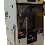
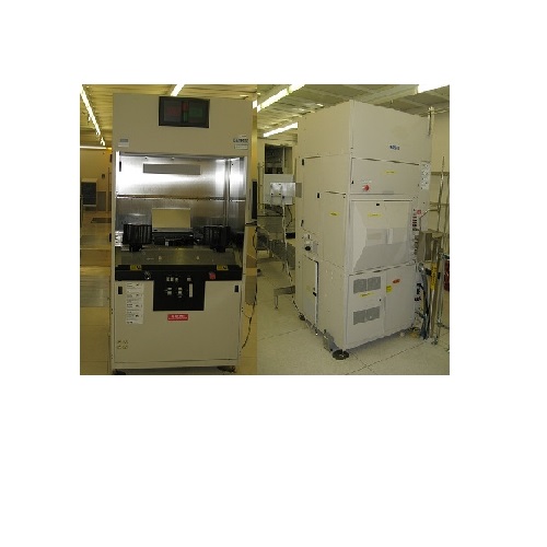
Model: Heatpulse 4100S
Category: RTP – Rapid Thermal Processing
Original Equipment Manufacturer: AG Associates
Condition: Used, Complete, working condition. Fully Refurbished and Tested by seller
Valid Time: Subject to prior sale
Lead Time: TBD
Location: Silicon Valley, CA, U.S.A.
Warranty: TBD,EXWORKS.
Others: Stainless Steel chamber (No chamber corrosion issues) and double O Ring front flange(For O2 sensitive processes).
Installation and training: Available at extra charge
Service Contract: Available at extra charge
AG Associates Heatpulse 4100S Rapid Thermal Processing equipment description
The AG Associates Heatpulse4100S rapid thermal anneal system contains a subsystem for each of the following:
• Electronics (including a dedicated microprocessor)
• Mass-flow-controlled gas handling
• Cooling
• ULPA filtration
• Mechanical assemblies
Software programs, called recipes, specify the details for each process. The AG Associates Heatpulse 4100S system includes a 3-1/2-inch floppy disk drive for process recipe storage. A three-axis industrial robot automates processing by transporting wafers into and out of the process chamber. It uses closed-loop feedback for precise motion control and accurate positioning.
To provide cold-wall processing, water is circulated through the process-chamber walls. The quartz isolation tube is cooled with nitrogen or compressed air.
AG Associates Heatpulse 4100S Rapid Thermal Anneal equipment APPLICATIONS:
The Heatpulse 4100S system is a versatile tool which can be useful for many applications, such as (but not limited to):
• Silicon dielectric growth
• Implant annealing
• Glass re-flow
• Titanium compound materials annealing
• Nitridation of metals
• Contact alloying
• Oxygen donor annihilation
AG Associates Heatpulse 4100S Rapid Thermal Processing Equipment Specifications:
Operating Specifications
The following are the operating specifications for the Heatpulse® 4100S system.
-
- Wafer handling: automatic serial processing, using standard cassettes.
- Throughput: Process dependent, approximately 80 wafers per hour (in a null cycle) without flat-finder.
- Stainless Chamber
- Wafer sizes: 3 inches, 4 inches, 5 inches, 6 inches (standard).
- Ramp-up rate: Programmable, 1 – 180°C per second.
- Steady-state duration: 1 – 600 seconds per step.
- Ramp-down rate: Programmable, 1 – 180°C per second. Ramp-down rate is temperature and radiation dependent, maximum 150°C per second.
- Recommended steady-state temperature range: 400 – 1200°C.
- ERP temperature accuracy: +5°C to -9°C, when calibrated against an instrumented thermocouple wafer (ITC).
- Temperature repeatability: + 7°C or better at 1150°C wafer to wafer. (Repetition specifications are based on a 100-wafer set.)
- Temperature uniformity: + 10°C across an 6-inch wafer at 1150°C. (This is a 1-sigma deviation from 100-angstrom oxide uniformity.) For a titanium silicidation process, no more than 1.5 percent increase to uniformity during the first anneal at 650 – 700°C.
AG Associates Heatpulse 4100S Physical Dimensions
-
- Width: 52 in. (102 cm)
- Depth 42 in. (107 cm)
- Height 82 in. (208 cm)
- Weight:: 1800 lbs (816 kg)
- Shipping weight:: 2000 lbs (907 kg)
AG Associates Heatpulse 4100S Utility Requirements
-
- Power StandardWater Type Refer to the Heatpulse® 4100 Facilities Manual.(Recirculator)
- Domestic: 208 VAC, 60 Hz; 125 A maximum;3-phase plus ground and neutral
- European: 400 VAC, 50 Hz; 90 A maximum;3-phase plus ground and neutral
- Japanese: 200 VAC, 50/60 Hz, 125 A maximum; 3-phase plus ground
- Power StandardWater Type Refer to the Heatpulse® 4100 Facilities Manual.(Recirculator)
AG Associates Heatpulse 4100S Rapid Thermal Anneal equipment FEATURES:
The AG Associates Heatpulse 4100S Rapid Thermal Annealing system contains many capabilities which provide significant advantages over conventional batch processing in the production of VLSI circuits. Cleanroom integrity, precise temperature control and measurement, software flexibility, and the physical structure of the system (designed for the production environment) are among these advantages.
- Contaminant-Free Processing
The Heatpulse 4100S system is designed with the cleanroom environment in mind. The following are the key features which make this Heatpulse 4100S system contaminant-free:
• Stainless-steel laminar flow processing floor and ULPA filter located in the processing area to reduce the number of particles in the environment. The walls of the processing area are also stainless steel.
• Design which prevents particles from circulating around the wafer-handling area, which allows the front panel door to remain open during processing.
• Easy service access available from rear and side panels.
• Through-the-wall installation, which maintains cleanroom integrity.
• No belts and pulleys (a large source of particle contamination) exist in the 8108 wafer-handling area.
• Front touch-screen controller remotely mounted to further reduce particle attraction.
- Heating, Cooling, and Temperature Measurement
The following lists the key features of Heatpulse 4100S heating, cooling, and temperature measurement:
• High-intensity radiation which heats wafers for short periods of 1 to 600 seconds at precisely controlled temperatures in the 400-to-1200°C range.
• Tungsten halogen lamps and cold process-chamber walls which allow fast wafer heating and cooling rates, respectively.
• Lamps arranged in 2 banks of 14 lamps each, 1 bank above and the other below the process chamber. Upper lamps which run crosswise and lower lamps which run lengthwise. Thus, the upper and lower lamps are at right angles to each other for optimization of temperature control. In addition, 10-zone lamp control to enable further wafer uniformity.
• The system delivers time and temperature profiles tailored to suit specific process requirements.
• Pyrometer or thermocouple sensing which offers precise closed-loop temperature control.
• Open-loop intensity control (OLIC) option which offers accurate, repeatable temperature control. (This feature requires ±0.5 VAC at 208 VAC line voltage regulation to function accurately.)
• Purge gas which flows through the process chamber and cooling gas (CDA) which flows around the isolation tube and lamps.
• Water de-ionizing system for oven cooling water to minimize metal corrosion.
- Software
The AG Associates Heatpulse system features touch-screen operation which is easy to learn. Additional software features are listed below.
• Menu screens which allow a process cycle to be easily defined and executed.
• Status reports continually displayed on the screen as the system operates.
• Self-diagnostic routine active whenever the system is on and terminates the cycle in progress if an abnormal condition is detected.
• Access codes which provide security for the system, recipe programming, and diagnostic functions.
• Highly flexible recipes and process procedures.
• Simple and easy-to-use menu screens.
• Touch-screen menus which eliminate the need for special commands.
• Manual mode which allows engineers and service personnel to activate individual subassemblies and functions.
• Discrete diagnostic routines, using a separate Diagnostic mode, are available.
• Maintenance menu which allows you to customize messages by condition and date to appear on the GUI screen at a set time.
• Thermal processing cycles which may be customized for unique processing requirements.
• Custom recipes created by process engineers which may be saved on floppy diskette and executed by production line operators.
- Service Access
The AG Associates Heatpulse 4100S system has been built for fast servicing in the production environment which provides low mean time to repair (MTTR ). The features listed below reflect this purpose:
• Optional menu screen available at the rear of the system, enabled through a key control switch.
• Gas box specifically designed for easy access and maintenance.
• Front access window closes to prevent cleanroom contamination during maintenance for through-the-wall installation.
• Top window, which flips out of the way, enables easier wafer-handling area access.
- Wafer Handling, Control, and Accuracy
Heatpulse 4100S wafer-handling system features include the following:
• Consistent wafer-to-wafer process cycle repeatability
• Optional send and receive cassette bases which swivel to accommodate loading and unloading by a cleanroom robot in a fully robotic environment
• Antistatic Ion Bar in the laminar flow system which reduces electrostatic charges on wafer handling components.
• Controlled ambient
• Robotic transport of wafers in excess of 80 wafers per hour (in a null cycle without the flat-finder option)
• A process-per-wafer (PPW) feature which enables you to program a different recipe for each wafer in a cassette. For pick-and-place operation, one recipe and be selected for each cassette, or up to 50 different recipes can be programmed when two 25-slot cassettes are used, or 52 recipes when two 26-slot cassettes are used
All the Heatpulse 4100S Rapid Thermal Processing , Rapid Thermal Annealing equipment trademarks belongs to AG Associates , the original equipment manufacturer. All rights reserved.
Rapid Thermal Processing and Rapid Thermal Anneal Introduction Rapid thermal processing (or RTP) refers to a semiconductor manufacturing process which heats silicon wafers to high temperatures (up to 1200 C or greater) on a timescale of several seconds or less. The wafers must be brought down (temperature) slow enough however, so they do not break due to thermal shock..Such rapid heating rates are attained by high intensity lamps process. These processes are used for a wide variety of applications in semiconductor manufacturing including dopant activation, thermal oxidation, metal reflow and chemical vapor deposition.Rapid thermal anneal (RTA) is a process used in semiconductor device fabrication which consists of heating a single wafer at a time in order to affect its electrical properties. Unique heat treatments are designed for different effects. Wafers can be heated in order to activate dopants, change film-to-film or film-to-wafer substrate interfaces, densify deposited films, change states of grown films, repair damage from ion implantation, move dopants or drive dopants from one film into another or from a film into the wafer substrate. Rapid thermal anneals are performed by equipment that heats a single wafer at a time using lamp based heating that a wafer is brought near. Unlike furnace anneals they are short in duration, processing each wafer in several minutes. Rapid thermal anneal is a subset of processes called Rapid Thermal Process (RTP).Rapid thermal processing (or RTP) refers to a semiconductor manufacturing process which heats silicon wafers to high temperatures (up to 1200 C or greater) on a timescale of several seconds or less. The wafers must be brought down (temperature) slow enough however, so they do not break due to thermal shock..Such rapid heating rates are attained by high intensity lamps process. These processes are used for a wide variety of applications in semiconductor manufacturing including dopant activation, thermal oxidation, metal reflow and chemical vapor deposition.Rapid thermal anneal (RTA) is a process used in semiconductor device fabrication which consists of heating a single wafer at a time in order to affect its electrical properties. Unique heat treatments are designed for different effects. Wafers can be heated in order to activate dopants, change film-to-film or film-to-wafer substrate interfaces, densify deposited films, change states of grown films, repair damage from ion implantation, move dopants or drive dopants from one film into another or from a film into the wafer substrate. Rapid thermal anneals are performed by equipment that heats a single wafer at a time using lamp based heating that a wafer is brought near. Unlike furnace anneals they are short in duration, processing each wafer in several minutes. Rapid thermal anneal is a subset of processes called Rapid Thermal Process (RTP).Rapid thermal processing (RTP) provides a way to rapidly heat wafers to an elevated temperature to perform relatively short processes, typically less than 1-2 minutes long. Over the years, RTP has become essential to the manufacture of advanced semiconductors, where it is used for oxidation, annealing, silicide formation and deposition.An RTP system heats wafers singly, using radiant energy sources controlled by a pyrometer that measures the wafer’s temperature. Previous thermal processing was based on batch furnaces, where a large batch of wafers is heated in a tube. Batch furnaces are still widely used, but are more appropriate for relatively long processes of more than 10 minutes.RTP is a flexible technology that provides fast heating and cooling to process temperatures of ~200-1250??C with ramp rates typically 20-200??C/sec, combined with excellent gas ambient control, allowing the creation of sophisticated multistage processes within one processing recipe. This capability to process at elevated temperatures for short time periods is crucial because advanced semiconductor fabrication requires thermal budget minimization to restrict dopant diffusion. Replacement of the slower batch processes with RTP also enables some device makers to greatly reduce manufacturing cycle time, an especially valuable benefit during yield ramps and where cycle-time minimization has economic value.RTP systems use a variety of heating configurations, energy sources and temperature control methods. The most widespread approach involves heating the wafer using banks of tungsten-halogen lamps because these provide a convenient, efficient and fast-reacting thermal source that is easily controlled. In a typical RTP system , the wafer is heated by two banks of linear lamps ?a one above and one below it. The lamps are further subdivided into groups or zones that can be individually programmed with various powers to maximize temperature uniformity. In RTP, the energy sources face the wafer surfaces rather than heating its edge, as happens in a batch furnace. Thus, RTP systems can process large wafers without compromising process uniformity or ramp rates. RTP systems frequently incorporate the capability to rotate the wafer for better uniformity.An important RTP application is the activation of ion-implanted dopants to form ultrashallow junctions. This requires fast ramp and cooling capabilities because the wafer must be heated to ~1050??C to anneal out ion implantation damage and activate the implanted dopant species. However, the time at temperature must be reduced to minimize diffusion. This has led to the spike-anneal approach, where the wafer is ramped to a high temperature and then cooled immediately.Another indispensable RTP application is in the formation of silicides. In this process, metal films react with the silicon on source/drain and gate regions to form silicides. In advanced logic processes, the metal is usually cobalt, but nickel is being explored for the 65 nm node. Silicide formation processes are usually performed at <500??C, and wafers must be kept in a very pure gas ambient because metal films can be sensitive to oxidation. RTP systems are ideal, because they have small chamber volumes easily purged with high-purity gas, creating a very clean environment.RTP is also increasingly important in oxidation applications, where the capability to use short process times at high temperatures and a wide variety of gas ambients provides excellent quality films and superior process control. RTP-grown oxides are often used for gate dielectrics, tunnel oxides and shallow-trench isolation liners. The use of steam in the gas ambient has opened new RTP applications. One of special interest for advanced DRAM technology is the use of a hydrogen-rich steam ambient for selective oxidation of gate stacks that include tungsten.Recently, RTP-like processing has found applications in another rapidly growing field ?a solar cell fabrication. RTP-like processing, in which an increase in the temperature of the semiconductor sample is produced by the absorption of the optical flux, is now used for a host of solar cell fabrication steps, ncluding phosphorus diffusion for N/P junction formation and impurity gettering, hydrogen diffusion for impurity and defect passivation, and formation of screen-printed contacts using Ag-ink for the front and Al-ink for back contacts, respectively.Some solar cell companies have successfully applied our advanced Rapid Thermal Processing (RTP) technology to its process for creating highly efficient and durable CIGS solar cells. This eliminates a key process bottleneck found in many state-of-the-art process implementations and enables the use of low-cost substrates in ways that were not considered possible before.In Rapid Thermal Processing, a layer is heated for a very brief period only in a highly controlled way. For instance, RTP techniques can flash-heat a layer for just several picoseconds and put energy just into the top several nanometers of a layer in a highly controlled way — while leaving the rest of the layer unaffected.RTP has a secondary benefit of reducing the energy payback time of their solar cells to less than two months (for the full panel). By comparison, a typical silicon solar panel has an energy payback time of around three years, and a typical vacuum-deposited thin-film cell has one of 1-2 years. The energy payback time is the time that a solar panel has to be used in order to generate the amount of energy that it required to be produced.