Description
Typical NANOTECHNOLOGY Lab Fab Equipment
Please contact us for our Main Refurbished Equipment. Appreciate your time.
The trademarks of the equipment and parts contained in this website belonged to the Original Equipment Manufacturers.
|
Mask Making Equipment: A photomask is typically a transparent fused glass blank covered with a pattern defined by chrome metal. A set of photomasks, each defining a pattern layer in nanoelectronic fabrication, is fed into a photolithography contact aligner or stepper and individually selected for exposure on a silicon wafer. In the case of the contact aligner, there is a one-to-one correspondence between the mask pattern and the wafer pattern. With the stepper, however, the pattern is projected and shrunk by five times onto the wafer surface. |
||
| Heidelberg DWL 2000 Laser Lithography System | 1. Environment chamber, providing a stable environment for the system – Laminar airflow (adjustable): 0.3 – 0.5 m/s – Temperature stability: ± 0.1 °C – Air quality: Class 10 2. Stage system with linear motors, air bearings and interferometric position control – Maximum substrate size: 9″ x 9″ – Maximum write area: 200 x 200 mm² (min. 5 mm from substrate edge) – Substrate thickness: 0 to 7 mm 3. Writing performance – Write mode: I and II – Minimum feature size: 0.5um , 0.7um – Edge roughness(3s): 40nm , 50nm – CD uniformity(3s): 60nm , 80nm – Alignment measurement accuracy(3s): 60nm, 70nm – Overlay accuracy(3s): 160nm, 200nm – Write speed (mm2/minute): 29, 110 |
|
| JEOL JBX-6300FS E-Beam Lithography System | Writing Mode : High speed or high precision Beam Current : 30pA to 20nA Scanning Speed : 12M to 250 Hz Accelerate Voltage : 20, 50 or 100 kV Max. Field Size (um2) : High speed mode: 2000 (20kV), 1000 (50kV) or 500 (100kV); High precision mode: 250 (20kV), 125 (50kV) or 62.5 (100kV) Mask : 5” x 5” x 0.09” Wafer : 4” or 2” Nano-imprint Mask : 65mm x 65mm x 6.35mm Chip Sample : 2cm x 2cm, 1.5cm x 1.5cm or 1cm x 1cm |
|
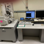
| Scanning Electron Microscope JEOL JSM-6490 | Resolution : HV mode 3 nm (30kV), 15 nm (1kV) LV mode 4 nm (30kV) Magnification : x8 to x300000 (at 11kV or higher) x5 to x300000 (at 10kV or lower) Specimen Stage : X :125mm, Y: 100mm, Z:5-80mm Tilt : -10 to +90 degree Image mode : Secondary electron image Accelerating Voltage : 0.3kV to 30kV Filament : Factory pre-centered filament Auto functions : Focus, brightness, contrast, stigmator Motor control : 5 axes computer controlled Frame store : 640 x 480, 1280 x 960 pixels Image format : BMP, TIFF, JPEG |
|
| Scanning Electron Microscope HITACHI TM4000Plus | Magnification : 10x-100,000x Specimen Stage : X: 40 mm, Y: 35 mm, Rotation: 0-360 degree Stage Control : Camera navigation System, 3 axes (X, Y, Rotation) computer controlled Max. Sample Size : 80 mm (dia.), 50 mm (thickness) Vacuum Mode : HV, LV Signal Detector : BSE detector, High-Sensitivity Low- Vacuum SE detector Image Signal : BSE, SE or Mix (BSE + SE) Image Adjustment : Auto start, Auto focus, Auto brightness, Camera Image Data Saving : 2,560 x 1,920, 1,289 x 960, 640 x 480 pixels Image Format : BMP, TIFF, JPEG |
|
|
Photolithography Equipment: Photolithography is the complicated process of transferring a pattern from a mask onto the surfaces of silicon wafers or any other substrates. Photolithography is in fact a highly refined version of photoengraving and is performed in a particle-free environment (the “yellow area”). The pattern is first transferred from the mask to a light-sensitive material called a photoresist. It is then transferred from the photoresist to the barrier material on the surface of the wafer by chemical etching or plasma etching. |
||
| Nanoscribe 3D Printer | Resolution (depends on the objective lens and resist) : – 3D lateral feature size: ≤200 nm – 2D lateral resolution: ≤500 nm – Vertical resolution: ≤1,500 nm Speed : – Beam scanning speed: 10 mm/s – Piezo scanning speed: 100 µm/s Range : – Motorized xy scanning stage range: 100 x 100 mm² -x-y-z piezo range: 300 x 300 x 300 µm³ -x-y galvo scan range 200 – 1000 µm Ø dependent on scanning objective Maximum structure height : – IP-Q 10x lens DiLL: 8 mm – IP-S 25x lens DiLL: 3 mm – IP DiP 63x lens DiLL: 3 mm – Oil immersion with 170 µm glass: 150 µm Minimum feature size : -10x lens: ~2 µm x, y and ~10 µm z -25x lens: 0.6 µm x, y and ~3.3 µm z -63x lens: 150 nm x, y and 800 nm z Objectives : 1. Immersion Objective: 63x, NA=1.4; WD=190 um, for high-resolution structures, printing field (Galvo Ø) = 200 um; Typical slicing distance = 0.3 µm; Typical hatching distance=0.2 µm2. Immersion Objective: 25x; NA=0.8; WD=380 um, for mesoscale structures; Printing field (Gavle Ø) = 400 µm; Typical slicing distance =1 µm; Typical hatching distance=0.5 µm3. Air Objective: 20x, NA=0.5; WD=2100 um, for 2D maskless lithography; Printing field (Galvo Ø) = 600 µm; Typical slicing distance=3-6 µm; Typical hatching distance= 0.7-1.2 µm4. Immersion Objective: 10x, NA=0.3; WD=700 um, for rapid prototyping; Printing field (Galvo Ø) =1000 µm; Typical slicing distance= 5 µm; Typical hatching distance =1 µm |
|
| ASML Stepper | Light source illumination : i-line (365 nm) Resolution : 0.5 µm Overlay alignment accuracy : ± 0.1 µm (3 sigma) Wafer size : 4″ or 6″ Field size : 15 mm x 15 mm or 10 mm x 10 mm (on wafer) Reduction ratio : 5:1 Photomask size : 5″ square |
|
| Karl Suss Bonder XB8 | Adhesive, Anodic, Eutectic bonding and Silicon fusion prebonding Wafer size : > 2 cm x 2 cm, 4″, 6″ & 8″ Substrate material : Silicon or Pyrex Glass Pressure : 1x10e-5 mbar to 3 bars Bonding force : 3500 N ~ 100K N (8″) Temperature : RT to 500 ºC Controllable Voltage range : 0 – 2000 V Controllable Current range : 0-15 mA |
|
| SET ACCµRA100 Flip-Chip Bonder | Flip-chip/Die bonding Substrate size : 1 mm x 1 mm to 100 mm x 100 mm Chip size : 1 mm x 1 mm to 50 mm x 50 mm Post-bonding accuracy : +/- 0.5 µm Bonding force : 1 N to 1000 N Temperature : RT to 400 ºC |
|
| Karl Suss MA6, 2 sets. | Light source illumination : i-line (365 nm) Resolution : 1 um Substrate size : > 5 mm2 to 2″ or 4” Photomask size : 5” square Exposure modes : Contact (soft, hard, low vacuum and Vacuum) Proximity (exposure gap 1-300um); Flood Exposures Alignment methods : Top Side Alignment (TSA); Bottom Side Alignment (BSA) Alignment accuracy : TSA (down to 0.5 µm); BSA (down to 1 µm) |
|
| AB-M Aligner (UV)/(DUV), 2 sets | Light source illumination : DUV / UV wavelength selectable (500W Mercury DUV lamp) Alighment printing mode : Manual Soft contact : Contact vacuum adjustable Hard contact : Full vacuum contact Photomask : 5″ square or 7″ square Substrate size : > 5 mm2 to 4″ square, or 6″ Special feature : Backside alignment using Infra-red |
|
| SVG88 Coater Track and SVG88 Developer Track, 2 sets | Automatic tracks for resist coating and developing No. of tracks : 2 Coat track feature : Vapor prime chill plate: Coat module Backside rinse: Frontside edge bead remover 2 hot plate ovens Develop track : Developer module, chill plate, 2 hot plate ovens Coating uniformity : ± 0.3 % Wafer size : 4″ and 6″ Wafer loading/unloading : Cassette to cassette |
|
| EVG Spray Coater | Speed range : up to 10000 rpm Ramp up speed : 0-40000 rpm/s Heat chuck temperature : up to 70 ± 1 oC Spray speed integrate with heat chuck : < 1500 rpm Spray coating nozzle : Ultrasonic Atomizer Nozzle Syringe dispense rate : 0.01 ml/s to 5 ml/s Substrate size : Up to 200 mm or 150 mm x 150 mm |
|
| SUSS Coater | Spin speed range : 0 to 7000 rpm Spin speed acceleration : 0-5000 rpm/s Coat system : Open Bowl; GYRSET Substrate size : > 5 mm2 to 6″ or 5″ square for single side coating 4″ for double side coating Other : Programmable bowl auto-clean; Edge bead remover |
|
| CEE Coater | Spin speed range : 0- 6000 rpm Spin speed acceleration : 0-30000 rpm/s Substrate size : 4″ or 6″ Other : Frontside edge bead remove |
|
| Desktop Coater | Spin speed range : 0 to 5000 rpm Substrate size : > 5 mm2 to 4″ square |
|
| Solitec Coater | Spin speed range : 250-5000 rpm Spin speed acceleration : 1000-4000 rpm/sec Substrate size : Larger than 5mm, 2 to 4″, 5″ square for single side coating or 4″ for double side coating |
|
| High Temperature Conventional Oven, 8 sets | High temperature oven : Up to 450 oC Convention oven temperature : Up to 250 oC Substrate size : Up to 6″ |
|
| Vacuum Oven | Temperature : Up to 300 oC Substrate size : 1 cm2 to 4″ Vacuum : 0 to 30 in.Hg Other : N2 purge |
|
| Unitemp Reflow Oven ,2 sets (Flip-Chip Bonder too) | Reflow Soldering (with Formic Acid Option) Substrate size : Fragments to 160 mm Substrate Thickness : Up to 10 mm Vacuum Range : Atmosphere to 10-3 hPa or mbar Oven Temperature : Ambient to 350oC Ramp Up Rate : Up to 120 K/min Gas Flow Control : Nitrogen at max. 5 normal litre per min |
|
| Nikon IC Inspection Microscope with Digital Camera | Contrast methods : BF /DF/ DIC/ Fluorescence Magnification : 50X – 1500X Wafer holder : up to 6″ Mask holder : 5″ square Digital camera : 5M pixel CCD Display : 8.4″ TFT LCD XGA Software : Dimension measurement tool |
|
| Hot Plates , 8 sets | Computer temperature controller with digital readout Substrate size : Up to 6″ Temperature : 50 to 250 oC Temperature uniformity : ± 1 oC |
|
| Laurell PDMS Coater (Microfluidic) | Spin Speed range : 0- 6000 rpm Spin speed acceleration : 0-30000 rpm/s Substrate size : 2″ or 4″ |
|
| Kurabo PDMS Mixer/Deaerator (Microfluidic) | Max. processing quantity : 310 g x 1 container Revolution : 200 – 2000 rpm (Mixing mode) 400 -2200 rpm (Deaerate mode) Rotation : Max 800 rpm (Mixing mode) Max 66 rpm (Deaerate mode) Setting time : 0 – 30 mins x 9 steps |
|
|
Wet Etching and CMP Equipment : Chemical wet etching is the technique of removing any barrier material not protected by the hardened photoresist after the photolithography process using liquid-phase etchants. Etchants must be highly purified and filtered. Which etchant to use depends on the material to be etched. We have several specially designed wet processing stations and a wide variety of pre-mixed etchants to choose from. The Chemical and Mechanical Polishing (CMP) process is a breakthrough technology in the manufacture of today’s advanced semiconductor chips. It is a highly accurate process of flattening and smoothing the surface of a silicon wafer so that multiple layers of intricate chip circuitry can be built on it. The process is essential to maintaining a wafer’s integrity, especially as the new generations of chips continue to shrink in size. |
||
| Wetstations, 10 sets | Silicon Etch using KOH / TMAH (25%) Photoresist Strip / ITO Etch Aluminum Etch / Pad Oxide Etch Oxide / Nitride Etch Wafer Cleaning (RCA) Wafer Cleaning (Piranha Clean) Solvent Cleaning |
|
| Wetstation , 3 sets | MS2001 Resist Stripper FHD5 Manual Developer Quick Dump Rinsers Small samples up to 6” |
|
| Wetstation | Hydrochloric Acid Etch Prior E-Beam Metallization DI Water Gun for rinse N2 Gun for dry Small samples up to 6″ |
|
| Wetstation , 8 sets | MS2001 resist stripper FHD5 manual developer Quick dump rinsers Small samples up to 6″ |
|
| USI Wafer Cleaner | Wafer surface scrubbing for pre-CMP and post -CMP process Fully automatic microprocessor control Completely enclosed chamber for washing, rinsing and drying 4″ wafer cleaning 9″ brush travel |
|
| Silicon Grinder | Mechanical grind for Silicon Oxide or Silicon using diamond wheel >5mm2 to 4″ wafer size 100-800um wafer thickness |
|
| Buehler Polisher | Polished for Silicon, Silicon Oxide or Silicon Nitride >5mm2 to 4″ wafer size 100-800um wafer thickness |
|
| Buehler Polisher | Polished for Copper, CNT, Silicon, Silicon Oxide or Silicon Nitride >5mm2 to 4″ wafer size 100-800um wafer thickness |
|
| GnP CMP | Equipment model : POLI-400L Polishing materials : Silicon dioxide or Polysilicon Sample Size : 1″x1″ or 4″ Wafer Thickness : 400-550 µm Wafer Carrier : Membrane style with floating ring Polishing platen and wafer carrier speed range : 30-200 rpm Oscillating Arm Pad Conditioning |
|
| Copper Electroplating | Copper Electroplating on 2″ single side or 4″ single/double sides wafer size Ready for Copper Electroplating to fill the small trench 300-550um wafer thickness |
|
|
Thermal Diffusion and Ion Implantation Equipment : To fabricate nanostructures and nanodevices, various kinds of thin films are used. Thermal oxidation plays an important role in silicon device fabrication. It is a key process in modern semiconductor technology. Dielectric materials, such as silicon dioxide and silicon nitride, are mainly used for insulation and passivation. Low-Pressure Chemical Vapor Deposition (LPCVD) and Plasma-Enhanced Chemical Vapor Deposition (PECVD) are the most commonly used methods for thin film deposition. For high-K material, atomic layer deposition offers precise control of film thickness down to the atomic scale and excellent conformity even in high-aspect-ratio structures. Polysilicon acts as the gate electrode and device interconnection is achieved through silicide formation. The thermal process facilitates oxidation and thin film deposition in wafer processing. Other related processes are thermal annealing which enables us to study the properties of different materials or their structural performance as a function of temperature, thermal diffusion dopant activation, etc. Ion implantation is the process by which impurities such as boron and phosphorous are introduced into a silicon wafer to control the majority-carrier type and resistivity of layers formed on the wafer. It is the primary method used to modify the electrical properties of wafers. Following ion implantation, a thermal diffusion or annealing process is needed to drive-in and activate the implanted dopants. |
||
| CF-3000 Implanter ,IMP-3000 | Dose Energy : 10 to 180 keV Max. Dose (ion/cm2 ) : 1016 Processing : Arsenic, Phosphorus, Boron, BF2 & Hydrogen implant |
|
| LPCVD,7 sets | Each deposition has its programmed flow of gases compositions, temperature and pressure ASM LB45 LPCVD Furnace: Polysilicon, Amorphous silicon, N-doped Amorphous Silicon, Silicon Germanium, Silicon Nitride, Low Temperature Oxide (LTO), Phosphorous Silicon Glass (PSG) Flokal LPCVD Furnace: Polysilicon, Amorphous silicon, Silicon Nitride, Low Stress Silicon Nitride, LTO, PSG |
|
| Diff. Furnace , 9 sets | Operating temperature : 400 to 1150 oC Processing : Dry & Wet Oxidation with TCE, N/P diffusion, Forming Gas annealing and Drive in |
|
| ET3000 Epitaxy | Epitaxial layers of Silicon, Silicon Germanium, N-doped(PH3), P-doped (B2H6) Fit for up to a 4″ wafer |
|
| Surface Tech Sys ( STS , SPTS ) Multiplex STS PECVD | Processing : Silicon Dioxide, Silicon Nitride Silicon Oxynitride Amorphous Silicon |
|
| Surface Tech Sys ( STS , SPTS ) Multiplex 310PC PECVD | Processing : Silicon Dioxide, Silicon Nitride Silicon Oxynitride Amorphous Silicon |
|
| TEOS PECVD | TEOS PECVD (CVD-TEOS) | |
| Oxford ALD | Thermal and plasma ALD Processing : Aluminum Oxide (Al2O3) Zirconium Oxide (ZrO2) |
|
| CNT PECVD | Frequency : 2455 MHz Processing : CNT growth Temperature : 900 oc |
|
| MPT RTP-600S RTP | Steady-state temperature stability : ±2℃ in the range of 250-1150℃ Heating rate : 0-200℃/sec Cooling rate : 150℃ max/sec Steady state time : 1-600 sec |
|
| AG Associates Heatpulse 610 RTP | Operating temperature in the range of 400℃ to 1000℃ Ion implantation annealing Silicide formation Nitridation of thin gate, dielectrics & silicide PSG/BPSG reflow |
|
| Allwin21 AW610 RTP | Wafer handling : Manual loading of wafer into the oven, single wafer processing Wafer sizes : Small samples and 2″, 4″ and 6″ wafers Ramp up rate : Programmable, 10℃ to 80℃ per second Ramp down rate : Programmable, 10℃ to 80℃ per second Operating temperature in the range of 250℃ to 800℃ Ion implantation annealing Silicide formation, nitridation of thin gate, dielectrics & silicide, PSG/BPSG reflow |
|
|
Dry Etching ,Evaporator and Sputtering Equipment : Dry etching is one of the most critical processes in micro and nanofabrication. This process is also known as dielectric etching, polysilicon etching, or conductor etching, depending on the type of film that is removed from the substrate. Two basic steps are involved. In the pattern definition step, a lithography process is used to create the desired pattern on the photoresist. Then in the pattern transfer step, the required pattern is dry etched onto the silicon itself, or onto a deposited layer of insulating or conducting material. The most common form of dry etching is reactive ion etching (RIE), through which a highly anisotropic profile of the etched material can be obtained. In-line process characterization for photolithography, etching, CMP, ion implantation and CVD enables us to monitor the machine performance and a number of key process control functions. We are equipped with many metrology systems providing non-destructive or destructive, real-time measurement of critical parameters. The effectiveness of the whole process can thus be monitored. |
||
| Surface Tech Sys ( STS , SPTS ) Multiplex Poly Etcher | Gases available : HBr, Cl2, O2, N2, He & Ar RF power source : 1x 1000W(max) at 13.56MHz for Coil electrode, 1x 300W(max) at 13.56MHz for Platen electrode Electrode coolant system : 20 oC High speed turbo molecular pump : pumping speed of 1000 L/s at 36000 rpm Fully automatic loadlock transfer system Substrate size : 4” single wafer Polysilicon etch Minimum line/space : 0.5 µm Low rate polysilicon etch E/R : ~ 900 Ȧ/min Selectivity to oxide : 13:1 Selectivity to photoresist : 12.5:1 Uniformity : 5% Normal rate polysilicon etch E/R : >1800 Ȧ/min Selectivity to photoresist : 2.5:1 Uniformity : 5% |
|
| Surface Tech Sys ( STS , SPTS ) Multiplex GaN Etcher | Gases available : BCl3, Cl2, CH4, SF6, O2, He & Ar RF power source : 1x 1000W(max) at 13.56MHz for Coil electrode, 1x 300W(max) at 13.56MHz for Platen electrode Electrode coolant system : 5 to 30 oC High speed turbo molecular pump : pumping speed of 1000 L/s at 36000 rpm Fully automatic loadlock transfer system Substrate size : 2″, 4″ or 6” single wafer or specimens GaN etch E/R : ~5000 Ȧ/min Selectivity to oxide : 10:1 Sapphire etch E/R : ~700 Ȧ/min Selectivity to oxide : 1.5:1 |
|
| Surface Tech Sys ( STS , SPTS ) Multiplex DRIE Etcher, Bosch Process | Gases available : C4F8, SF6, O2, N2, He & Ar RF power source : 1x 1000W(max) at 13.56MHz for Coil electrode, 1x 300W(max) at 13.56MHz for Platen electrode Electrode coolant system : 5 to 30 oC High speed turbo molecular pump : pumping speed of 1000 L/s at 36000 rpm Fully automatic loadlock transfer system Substrate size : 4″ wafer Silicon etch Minimum Line/Space : 0.5 µm Low Rate Silicon Etch E/R : From 500 Ȧ/cycle Normal Rate Silicon Etch E/R : Up to 2 µm/min Selectivity to Photoresist : >50:1 Selectivity to Oxide : >80:1 Uniformity : 7% |
|
| Surface Tech Sys ( STS , SPTS ) Multiplex DRIE Etcher Bosch Process | Gases available : C4F8, SF6, O2, N2, He & Ar RF power source : 1x 3600W(max) at 13.56MHz for Primary Source 1x 3000W(max) at 13.56MHz for Secondary Source 1x 200W(max) at 13.56MHz for Platen electrode 1x 200W(max) at 300-500kHz for Platen electrode Electrode coolant system : -20 to 40 oC High speed turbo molecular pump : pumping speed of 2350 L/s at 25000 rpm Fully automatic loadlock transfer system Substrate size : 4″ wafer Silicon etch Minimum Line/Space : 0.5 µm Aspect Ratio : Up to 60:1 Low Rate Silicon Etch E/R : From 0.7µm/min (700 Ȧ/Loop) Normal Rate Silicon Etch E/R : 2 µm/min Fast Rate Silicon Etch E/R : 18 µm/min Selectivity to Photoresist : From 12:1 to 250:1 Selectivity to Oxide : From 24:1 to 500:1 Uniformity : <5% |
|
| Surface Tech Sys ( STS , SPTS ) Multiplex DRIE Etcher | Gases available : C4F8, SF6, O2, N2, He & Ar RF power source : 1 x 1000W(max) at 13.56MHz for Coil electrode, 1 x 300W(max) at 13.56MHz for Platen electrode Electrode coolant system : 20 oC High speed turbo molecular pump : pumping speed of 1000 L/s at 36000 rpm Fully automatic loadlock transfer system Substrate size : 4″ wafer Silicon etch Minimum Line/Space : 1 µm Low Rate Silicon Etch E/R : 1 µm/min Normal Rate Silicon Etch E/R : Up to 2 µm/min Selectivity to Photoresist : >50:1 Selectivity to Oxide : >100:1 Uniformity : 7% |
|
| Surface Tech Sys ( STS , SPTS ) Multiplex AOE Etcher | Gases available : C4F8, CF4, CHF3, O2, N2, H2, He & Ar RF power source : 1x 3000W(max) at 13.56MHz for Coil electrode, 1x 600W(max) at 13.56MHz for Platen electrode Electrode coolant system : -5 to 30 oC High speed turbo molecular pump : pumping speed of 2000 L/s at 48000 rpm Fully automatic loadlock transfer system Substrate size : 4″ single silicon or quartz wafer Silicon Oxide etch Minimum Line/Space : 0.5 µm Silicon Oxide Etch E/R : AOE_PRD = 2300 Ȧ/min; AOE_PRB = 3000 Ȧ/min Selectivity to Photoresist : >4:1 Selectivity to Polysilicon : >15:1 Uniformity : 7.5% |
|
| PS210 Asher | Gases available : O2 & N2 Microwave power source : 2.45 GHz Substrate size : 4″ wafers |
|
| Branson/IPC 3000 plasma Asher | Gases available : O2 & N2 RF power source : 400W(max) at 13.56MHz Substrate size : 2″, 4″and 6″ wafers or specimens |
|
| Allwin21 AW-B3000 plasma Asher ,3 sets | Gases available : O2 & N2 RF power source : 400W(max) at 13.56MHz Substrate size : 2″, 4″ and 6″ wafers or specimens |
|
| Oxford RIE Etcher | Gases available : CHF3, SF6, O2, CF4, Ar, N2, He & H2 RF power source : 500W at 13.56MHz Huber electrode coolant system : -40 to 200 oC Substrate size : 4″, up to 3 wafers per run or specimen Silicon Dioxide Etch E/R : ~363 Ȧ/min for LTO E/R : ~352 Ȧ/min for thermal oxide Selectivity to photoresist : 2.6:1 Selectivity to Silicon Nitride : 0.8:1 Selectivity to Silicon : 6.7:1 Uniformity : 3.6% Silicon Nitride Etch E/R : ~810 Ȧ/min Selectivity to photoresist : 1.5:1 Selectivity to Silicon Dioxide : 2.1:1 Selectivity to Silicon : 5.4:1 Uniformity : 5.8% |
|
| AST Metal Etcher | Chlorine & Fluorine based barrel type system for etching aluminum Gases available : Cl2, BCl3, CF4, CHF3, He, Ar, O2 & N2 RF power source : 1000W(max) at 13.56MHz Bias power source : 1000W(max) at 13.56MHz Substrate size : 4″ wafers Aluminum Etch Al etch rate : 1700 Ȧ/min PR etch rate : 1000 Ȧ/min SiOx etch rate : 300 Ȧ/min |
|
| XeF2 Silicon Etcher | Gases available : XeF2 Substrate size : 2″, 4″ single wafer or specimens Silicon Etch Rate Bright field mask : 600 Ȧ/cycle Dark field mask : 6000 Ȧ/cycle Mask used : Oxide |
|
| Trion RIE Etcher | Gases available : CHF3, SF6, O2, CF4, Ar, N2, He and H2 ICP power source : 600W (max) at 13.56MHz RF power source : 600W (max) at 13.56MHz Electrode coolant system : 0 to 30 oC Substrate size : 4″, up to 3 wafers per run or specimens Silicon Dioxide Etch : ~500 Ȧ/min Silicon Nitride Etch : ~850 Ȧ/min |
|
| Oxford Aluminum Etcher | Gases available : Cl2, BCl3, HBr, CF4, SF6, O2 and Ar RF power source : 1 x 3000W (max) at 13.56MHz for coil electrode : 1 x 300W (max) at 13.56MHz for platen electrode Electrode coolant system : 5 to 60 oC High speed turbo molecular pump : pumping speed of 1250 L/s at 37800 rpm Fully automatic loadlock transfer system Substrate size : 4″ wafer Aluminum / Aluminum-Si etch Minimum line / space : 0.5 µm High rate Aluminum etch E/R : 3000 Ȧ/min Normal rate Aluminum etch E/R : 1800 Ȧ/min Selectivity to Photoresist : > 2:1 Selectivity to Oxide : > 10:1 Uniformity : 5% (etch from edge to center) |
|
| RIE Etcher | Gases available : CF4, CHF3, SF6 and O2 RF power : 120W Chiller temperature : 20 oC Fully automatic loadlock transfer system Substrate size : 4″ wafer Nitride etch rate : ~500 Ȧ/min Oxide etch rate : ~460 Ȧ/min Si etch rate : ~50 to 470 Ȧ/min Photoresist etch rate : ~151 to 400 Ȧ/min |
|
| Oxford GaN-InP Etcher | Gases available : Cl2, BCl3, CH4, H2, N2, SF6, O2, He and Ar RF power source : 1 x 3000W (max) at 13.56MHz for coil electrode : 1 x 600W (max) at 13.56MHz for platen electrode Electrode coolant system : -10 to 200 oC High speed turbo molecular pump : pumping speed of 1280 L/s at 39000 rpm Fully automatic loadlock transfer system Substrate size : 2″, 4″ or 6″ single full wafer GaN Etch E/R: : ~6000 Ȧ/min Selectivity to Oxide : 9:1 InP Etch E/R: : ~6000 Ȧ/min Selectivity to Oxide : 10:1 |
|
| Critical Point Dryer | Tousmis Automegasamdri®-915B, Series B Critical Point Dryer • Automatic Supercritical Point Dryer • All internal surfaces are inert to CO2 and ultra pure alcohols • 0.08µm internal filtration system delivers clean filtered LCO2 to process chamber • Small samples up to 6″ wafer • Up to five wafers per single process |
|
| Diener Plasma Cleaner | • Gases available: air • RF power source: 50 W (max) at 13.56 MHz • Substrate size: 2″, 4″ or specimens |
|
| Varian 3180 Sputterer | Gases available : Ar & N2 DC sputtering power source : 3 x 12KW RF back sputtering power source : 600W at 13.56MHz Fully automatic wafer handling system Substrate size : 4″ wafer Chamber pressure : 5 x 10⁻⁷ torr Target available : Mo, Pure Al, Al-Si & Ti Sputtering rate ( Ȧ/sec) ~160 Ȧ/sec for pure Al ~180 Ȧ/sec for Al/Si (1%) ~40 Ȧ/sec for Ti ~160 Ȧ/sec for Mo |
|
| CVC-601 Sputterer | Gases available : Ar & N2 DC sputtering power source : 1 x 3 KW RF sputtering power source : 1200W at 13.56MHz Chamber pressure : 5 x 10⁻⁷ torr Substrate size : 2″, 4″& 6″ wafers or 4″ square glass substrate Target available : Cu, TiW & Au Target available on request : Ti, Cr & Al-Si Sputtering rate (Ȧ/min): ~500 Ȧ/min for Al-Si ~175 Ȧ/min for TiW ~160 Ȧ/min for Au ~1000 Ȧ/min for Cu |
|
| ARC-12M Sputterer | Gases available : Ar, O2 & N2 DC sputtering power source : 2 x 250W RF sputtering power source : 600W at 13.56MHz Chamber pressure : 1.5 x 10⁻⁵ torr Substrate size : 2″, 4″ wafer or square glass, or specimens Target available : Ag, Al, Al/Si (1%), Au, Cu, Cr, Hf, Mo, Pt, Ti, TiW, Ni |
|
| CY1 Sputterer | Gases available : Ar, O2 & N2 DC sputtering power source : 1 x 500W RF sputtering power source : 1 x 500W (Currently unavailable) Chamber pressure : 5 x 10⁻⁶ torr Substrate size : 2″, 4″ wafer or square glass, or specimens Target available : Al, Ti, Cr, Al-Si, Ni, Mo, dielectric targets |
|
| Cooke Evaporator | Gases available : N2 E-beam power source : 1x 3KW Chamber pressure : 8 x 10⁻⁷ torr Substrate size : 2″ or 4″ wafers Source available (in Phase II) : Al, Ni, Mo, Ti, Cr |
|
| Cooke Evaporator | Gases available : N2 E-beam power source : 1x 3KW Chamber pressure : 8 x 10⁻⁷ torr Substrate size : 2″ or 4″ wafers Source available (in Phase III) : Al, Ni, Ti, Au, Cr, Pt, Fe, SiO2, Ag |
|
| AST 600EI Evaporator | Gases available : O2 and N2 E-beam power source : 2 x 6KW Chamber pressure : 9 x 10⁻⁸ torr Substrate size : 2″ and 4″ wafers or specimens Source available : Al, Au, Ti, Ni, Cr, Ge, Pt, Ag, ITO |
|
| AST 450I Evaporator | Gases available : N2 DC sputtering power source : 1 x 3KW Chamber pressure : 9 x 10⁻⁸ torr Substrate size : 2” wafer or specimens Source available : Al, Ti, Au & Ni |
|
| Edward Sputterer (Au) for SEM | Gases available : Ar RF power source : 100W at 13.56 MHz Chamber pressure : 1 x 10⁻³ torr Substrate size : 2″ and 4″ wafers or square glass, or specimens Target available : Au (For SEM only) |
|
| NSC3000 Sputterer | Gases available : O2, N2 & Ar DC sputtering power source : 1 x 1KW Chamber pressure : 5 x 10⁻⁶ torr Substrate size : 2″, 4″ wafer or square glass, or specimens Target available : Al, Ti, Cr, Al-Si, Ni & Mo |
|
| Metrology and Tester : In-line process characterization for photolithography, etching processes, CMP, ion implantation and CVD processes enables us to monitor the machine performance and a number of key process control functions. We are equipped with many metrology systems providing non-destructive or destructive, real-time measurement of critical parameters. The effectiveness of the whole process can thus be monitored. | ||
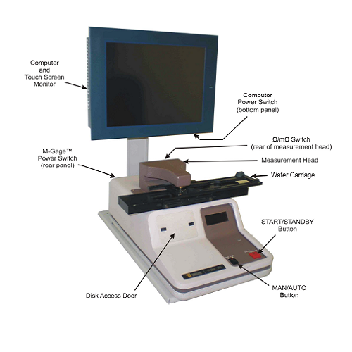
| Tencor Sono Gauge 300 | For single point measurement of wafer thickness, Aluminum film thickness and sheet resistance of metal Wafer Diameter : 3”, 4”, 5” and 6” Substrate Thickness : 250-700 µm Sheet Resistance : 1 to 1999 Ω/sq. Minimum Metal Film Thickness : 100 Ȧ |
|
| Tencor P-10 Surface Profiler | Measurement of roughness, waviness, step height on a surface Vertical Resolution : 1 Å (Max. vertical range 13μm), 25 Å (Max vertical range 300μm) Horizontal Resolution : 0.01 μm at 1μm/s scan speed Max. Scan Length : 60 mm, 2-D scan only Scan Speed : 1 μm/s to 25 mm/s Stylus Force : 1-100 mg Stylus Radius : 12.5 μm Display Magnification : 60-240x |
|
| KLA-Tencor P-7 Surface Profiler | Measurement of roughness, waviness, step height on a surface Vertical Resolution : 1 Å (Max. vertical range 13μm), 25 Å (Max vertical range 300μm) Horizontal Resolution : 0.025 μm Max. Scan Length : 150 mm, 2-D scan only Scan Speed : 2 μm/s to 25 mm/s Stylus Force : 0.5-50 mg Stylus Radius : 2 μm Display Magnification : 60-240x |
|
| Dektak 150 Veeco Surface Profiler | Measurement of roughness, waviness, step height on a surface Stylus Force : 1 to 15mg with LIS 3 sensor Stylus Radius : 2.5 μm and 12.5 μm Scan Length Range : 55mm Sample Stage : Manual Θ, 360° rotation, manual leveling, auto X-Y 150 mm travel, 1 μm repeatability, 0.5 μm resolution Data Points Per Scan : 60,000 maximum Max. Sample Thickness : Up to 100 mm Max. Wafer Size : 150 mm Step Height Repeatability : 6A, 1 sigma on 1μm step Vertical Range : 524 μm standard Vertical Resolution : 1A max. (at 6.55 μm range) |
|
| Four Dimension 280C Four-Point-Probe Mapping System | Range from 0.001 to 800k Ohm per square Single point, 5 points or external PC mapping measurement 3″ to 6″ wafer capability Various probe heads selection |
|
| Lucas Pro4-640R Resistivity Measurement System | Range from 0.001 to 800k Ohm per square 150 mm probe stand Keithley 2400 source meter Tungsten Carbide and Osmium probe heads Tip radius : 0.0016 inches Spring Pressure : 85 grams |
|
| NANOmetrics Nanospec AFT Model 4150 / 3000 | Single film thickness measurement on silicon substrate: Silicon Dioxide, Silicon Nitride, positive/negative photo resist and polymide Double layers measurement on Silicon substrate : Silicon Nitride on Silicon Dioxide, Polysilicon on Silicon Dioxide, Amorphous Silicon on Silicon Dioxide, Negative/positive resist on Silicon Oxide Standard visible system with Lens in 10x magnification Measuring light spot size : 15 μm (Model 4150) 25 μm (Model 3000) Automatic focusing and preset pattern of measurement point locations (Model 4150) |
|
| J.A. Woollam M-2000VI Spectroscopic Ellipsometer | Measure the optical constants: refractive Index, extinction coefficients and film Thickness for different materials Wavelength : 370 nm to 1690 nm, ~ 580 wavelengths All wavelengths are acquired simultaneously Focused beam diameter in ~200 μm Spectral resolution in 1.6 nm, 5 nm bandwidth Test Base fixed angle of 66°, horizontal sample stage for 100 mm wafer Automated z-height alignment |
|
| Atomic Force Microscope XE150S | Non-contact AFM imaging to investigate and analyze a sample surface Supports up to 6″ wafer 100 µm × 100 µm XY scan range Up to 12 µm Z scan range Radius of probe tip size, 10 nm Enhanced acoustic enclosure Fully motorized XY stage travels entire 150 mm × 150 mm |
|
| Film Stress Measurement System SMSi 3800 | Measure the change of curvature induced in a sample due to the deposited film on a reflected substrate Measure 1-D stress and produce 3-D topographical profile For wafer flatness and Pattern measurement Various of stress constant Wafer size : 2″ to 8″ Thickness limit : less than 11 mm Statistical process control and spreadsheet compatibility Automatic segmentation calculation |
|
| Keyence 3D laser confocal Microscope | Keyence VK-X260K 3D Laser Confocal Microscope provides non-contact, nanometer-level profile, roughness, and film thickness data on any material. Light source : 408nm violet laser source White light source Total magnification : Up to 28000x Optical microscope : Pinhole confocal optical system 4 Objectives (10X, 20X, 50X & 150X) Light receiving element : 16-bit photomultiplier Scanning method : Automatic upper/lower limit setting High-speed light intensity optimization (AAGII) Poor reflected light intensity supplement (Double Scan) Stage : Manual XY Stage 70mm×70mm Micrometric motorized Z translation Resolution : 1nm lateral resolution 0.5nm Z-axis movement of objective lenses Observation image : Super-high-resolution color CCD image 16-bit laser color confocal image Confocal + ND filter optical system C-laser differential interference image Sample size : Up to 5″ Maximum sample height 28mm |
|
| Perfict Lab Probe Station with Keysight B1500A Analyzer | Probing Stage: Sample size : Up to 152.4 mm (6 inch) Probe: Probe Tip Holder : Triaxle cable Current leakage: <50 fA Probe Tip diameter : 20 μm Stereo Microscope: Optical Magnification : 20X – 400X Keysight B1500A Semiconductor Device Parameter Analyzer: Current-Voltage (IV) measurement with 4 HRSMUs (High Resolution Source Monitor Units) Current range : ± 100 mA, measuring resolution 1 fA, sourcing resolution 5 fA Voltage range : ± 100 V, measuring resolution 0.5 μV, sourcing resolution 25 μV |
|
SS3499-20240524

