
Description
Universal X-RAY X-7900 ULTRA 3D/CT Inspection System (Brochure Download)
The X-7900 ULTRA is a high-precision 3D/CT open-tube X-ray inspection system designed for advanced semiconductor inspection, failure analysis, and high-resolution internal structure evaluation. It is suitable for universities, research institutes, and compound semiconductor fabs requiring 1 μm inspection capability, 160 kV penetration, and CT-based analysis for advanced materials and semiconductor devices.
Key Features
- 160 kV open X-ray tube for high-penetration inspection
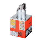
X-ray tube
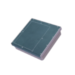
Detector
- 1 μm spatial resolution for high-precision semiconductor analysis
- 3D/CT capability supporting advanced internal structure inspection
- Planar CT and cone-beam CT capability for different inspection requirements
- Large 600 × 600 mm effective inspection area
- High-resolution flat panel detector with ±70° tilt capability
Strong Selling Points
- High-Resolution Semiconductor Inspection
The X-7900 ULTRA is designed for advanced semiconductor applications requiring fine defect detection, high image clarity, and precise internal structure analysis. - 160 kV Open-Tube Platform
The open-tube design provides strong inspection capability for dense materials, advanced packages, and compound semiconductor devices. - 1 μm Inspection Capability
With 1 μm spatial resolution, the system is suitable for high-precision applications including SiC, GaN, BGA, IGBT, flip-chip, TSV/TGV, and semiconductor failure analysis. - 3D/CT Analysis Capability
The system supports CT-based analysis, including planar CT and cone-beam CT, allowing users to evaluate complex internal structures beyond standard 2D X-ray inspection. - Strong Fit for Research and Advanced Material Labs
The X-7900 ULTRA is well suited for universities, research institutes, and advanced fabs that require higher resolution and deeper analysis capability than standard 2D inspection systems.
Applications
- Compound semiconductor inspection: SiC, GaN, III-V devices
- Advanced semiconductor packaging analysis
- BGA, IGBT, flip-chip, TSV/TGV, and IC package inspection
- Failure analysis and high-resolution defect inspection
- Battery, PCB, LCM display module, and advanced material inspection
- 3D/CT internal structure analysis
Positioning
The X-7900 ULTRA replaces the previous X-9200K listing as the high-end model in SemiStar’s X-ray inspection lineup. It is recommended for customers requiring the highest resolution, 160 kV capability, and 3D/CT analysis for advanced semiconductor and material inspection applications.
Specifications
| Category | Item | Specification |
| X-ray Source | Model | X-7900 ULTRA |
| Tube Type | Open tube | |
| Tube Voltage | 160 kV | |
| Tube Current | 500 μA | |
| Imaging | Spatial Resolution | 1 μm |
| Optical Magnification | 2000X | |
| System Magnification | 7500X | |
| Detector Resolution | 1536 × 1536 pixels | |
| A/D Density Value | 16 bit (65536) | |
| Frame Frequency | 20 FPS | |
| 3D / CT | CT Capability | 3D / CT inspection |
| CT Modes | Planar CT and cone-beam CT | |
| FPD Tilt Angle | ±70° | |
| Stage / Inspection | Stage Size | 670 × 670 mm |
| Sensing Range | 600 × 600 mm | |
| Load-bearing | ≤10 kg | |
| Stage Movement | Automatic / manual | |
| System | Operating System | Windows 11 |
| Power Supply | AC110–220V, 50–60Hz | |
| Power | 1200W | |
| Radiation Safety Test | <1 μSv/h | |
| Machine Size | 1578 × 1675 × 1910 mm (L × W × H) | |
| Machine Size Including Three-Color Light | 1578 × 1675 × 2265 mm (L × W × H) | |
| Machine Weight | 2200 kg |
* Specifications are for reference only and may vary depending on configuration. Please contact SemiStar or the manufacturer for official specifications.
Review how the X-7900 ULTRA compares with other X-ray inspection models in resolution, penetration, sample size, and application scope.
View full comparison →