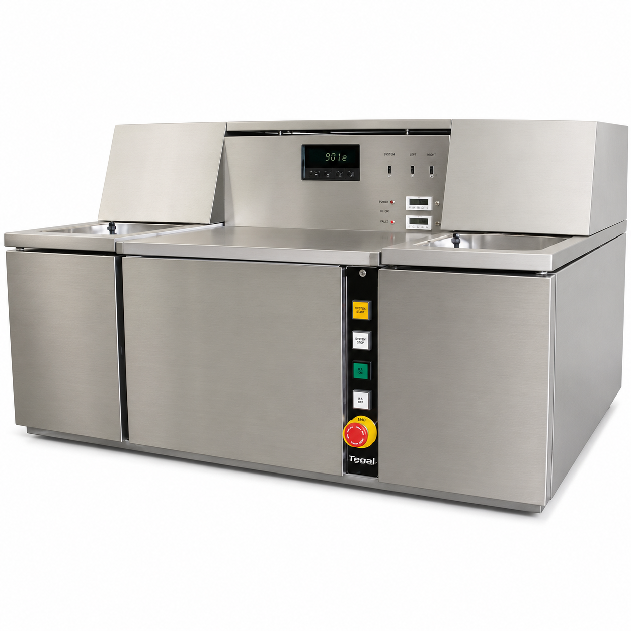
Description
Refurbished Tegal 903e Plasma Dry Etcher SiO2 Oxide Etch Semiconductor Equipment
SemiStar Corp. provides refurbished Tegal 903e plasma etcher systems for semiconductor oxide etching applications. The Tegal 903e platform is designed primarily for SiO2 oxide etching, SOG etching, and PECVD nitride topside etching applications for semiconductor manufacturing, universities, research institutes, and compound semiconductor fabs.
The Tegal 903e is different from the Tegal 901e platform. The Tegal 901e is mainly configured for polysilicon and SiNx nitride etching using SF6/O2 chemistry and different chamber/gap configuration, while the Tegal 903e is configured for oxide-based etching processes using CHF3, SF6, and Helium process gases with a different chamber structure and process tuning capability.
According to original Tegal training documentation, the Tegal 903e is configured as a diode reactor with approximately 6 mm electrode gap and supports oxide, SOG, and PECVD nitride topside etching applications using CHF3, SF6, and Helium process gases. Typical process pressure range is approximately 1600–3000 mTorr with RF power around 400–600 watts. :contentReference[oaicite:0]{index=0}
Photos shown are for reference only. Actual configuration, condition, and installed options may vary. OEM trademarks belong to their respective owners.
Availability
- Refurbished Tegal 903e plasma dry etcher systems
- Various configurations depending on availability
- 150 mm and 200 mm capability may be available depending on configuration
- Systems subject to prior sale
- Only for qualified end users
System Description
The Tegal 903e is a classic semiconductor plasma dry etcher platform widely used for oxide and dielectric etching applications. The platform has been used in semiconductor fabs, universities, and research institutes for SiO2 pattern transfer and dielectric processing applications.
Typical applications include:
- SiO2 oxide etching
- SOG (Spin-On Glass) etching
- PECVD nitride topside etching
- Semiconductor dielectric pattern transfer
- Research and process development
- MEMS and compound semiconductor applications
Typical Tegal 903e Process Configuration
- Reactor Type: Diode plasma etcher
- Typical Electrode Gap: ~6 mm
- Typical Wafer Size Capability: 3-inch to 6-inch
- Main Process Gases: CHF3, SF6, Helium
- Typical Process Pressure: 1600–3000 mTorr
- Typical RF Power: 400–600 W
- Typical Process Temperature: ~23°C
- Vacuum pump configuration depends on system
- Gas box and MFC quantity depend on configuration
Difference Between Tegal 901e and Tegal 903e
| Model | Main Application | Main Process Gases | Typical Reactor Gap |
|---|---|---|---|
| Tegal 901e | Polysilicon / SiNx Nitride Etch | SF6, O2 | ~38 mm |
| Tegal 903e | SiO2 Oxide / SOG / PECVD Nitride | CHF3, SF6, Helium | ~6 mm |
The Tegal 901e and 903e are not simply software differences. The chamber structure, process gap, gas configuration, and process optimization are different between the two systems.
Refurbishment Capability
SemiStar Corp. may provide refurbishment, repair, and upgrade support depending on the condition and configuration of the original system.
Possible support capability may include:
- RF generator and matching network evaluation
- Vacuum system refurbishment
- Gas delivery system inspection
- Chamber cleaning and refurbishment
- MFC replacement or calibration
- Controller and electronics repair
- PC-based controller upgrade options
- Touchscreen monitor upgrade options
- Data logging and GUI upgrade options
- Spare parts support depending on availability
Facility Requirements
- Process gases and gas cabinets are buyer responsibility
- Vacuum pumps and exhaust systems are buyer responsibility unless specifically quoted
- Cooling water, CDA, and facility connections are buyer responsibility
- Electrical requirements depend on final system configuration
- Facility preparation should be confirmed before shipment
Applications
- Semiconductor fabs
- Universities and research institutes
- MEMS device fabrication
- Compound semiconductor device processing
- Oxide dielectric etching applications
- Process development laboratories
Important Notes
- Configuration depends on actual available inventory
- Photos and specifications are for reference only
- Final specifications are subject to formal quotation
- Used/refurbished semiconductor equipment may show cosmetic wear
- Equipment availability subject to prior sale
- Customer is responsible for process qualification and application verification
RFQ Information Requested
- Wafer size and material
- Target process application
- Current process gases
- Existing tool model and configuration
- Required throughput
- Facility information
- Expected purchase timeline
- Special options or upgrade requirements