")

Description
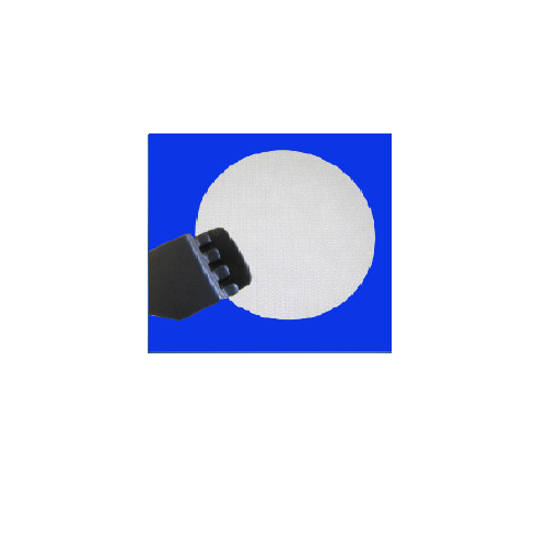
We are a high-tech company devoting to developing technologies to fabricate high-quality nitride semiconductor materials. Our key advantage is unrivaled materials expertise, and owns essential patents in GaN substrate and growth technologies. We offer Non Polar Freestanding GaN Substrate(a-plane and m-plane) with extra low dislocations densities,which are suitable for applications in high-power LED, blue and green LD, HEMTs, high-power electronic/electric devices.
Our mission is bringing key values to the related industries, such as full color display, semiconductor lighting, communication, and renewable energy, and being a pioneer in the industry applications of nitride semiconductors.
Non Polar Freestanding GaN Substrate(A-plane and M-plane) specifications
| Item | GaN-FS-A-U/N/SI-S | GaN-FS-M-U/N/SI-S | GaN-FS-SP-U/N/SI-S |
| Dimensions | 5.0~10.0 mm × 10.0 mm; ± 0.2 mm | ||
| 5.0~10.0 mm × 20.0 mm; ± 0.2 mm | |||
| Thickness | 350 ± 25 µm | ||
| Orientation | A-plane(11-20) off angle toward C-Axis -1°± 0.2° | M-plane(1-100) off angle toward C-Axis -1°± 0.2° | (20-21)
(20-2-1) (11-22) (30-31) (10-11) |
| TTV(Total Thickness Variation) | ≤ 10 µm | ||
| BOW | ≤ 10 µm | ||
| Conduction Type
Resistivity(300K) |
N-type(Undoped) < 0.5 Ω·cm | ||
| N-type(Ge-doped) < 0.05 Ω·cm | |||
| Semi-Insulating(Fe-doped) > 106 Ω·cm | |||
| Dislocation Density | 5×105 cm-2~3×106 cm-2 | ||
| Useable Surface Area | > 90% | ||
| Polishing | Front Surface: Ra < 0.2nm. Epi-ready polished
Back Surface: Fine ground |
||
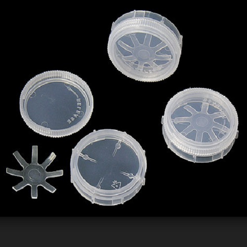
| Package | Packaged in a class 100 clean room environment, in single wafer containers, under a nitrogen atmosphere. | ||
Gallium nitride (GaN) is a binary III/V direct bandgap semiconductor commonly used in bright light-emitting diodes since the 1990s. The compound is a very hard material that has a Wurtzite crystal structure. Its wide band gap of 3.4 eV affords it special properties for applications in optoelectronic, high-power and high-frequency devices. For example, GaN is the substrate which makes violet (405 nm) laser diodes possible, without use of nonlinear optical frequency-doubling.
Its sensitivity to ionizing radiation is low (like other group III nitrides), making it a suitable material for solar cell arrays for satellites. Military and space applications could also benefit as devices have shown stability in radiation environments. Because GaN transistors can operate at much higher temperatures and work at much higher voltages than gallium arsenide (GaAs) transistors, they make ideal power amplifiers at microwave frequencies.