
Description
Silicon carbide coated graphite component products for semiconductor equipment:
ID-SS11129
Our partner specializes in the research, development, production, and sales of silicon carbide (SiC)–coated graphite components for semiconductor equipment, along with related coating services. Its products are designed for use in a wide range of semiconductor reaction chambers, including SiC epitaxy, MOCVD, and silicon epitaxy systems. These components and services are widely applied across the semiconductor and broader pan-semiconductor industries.
Driven by continuous process optimization and new product development, the company follows a strategy of “developing one generation, reserving one generation, and marketing one generation.” In addition to SiC-coated graphite components, it is actively developing advanced materials such as solid SiC parts for epitaxy, etching, oxidation/diffusion, and crystal growth processes, as well as sintered SiC components and tantalum carbide (TaC)–coated graphite parts, many of which are entering pilot production and validation stages. The company is committed to advancing key semiconductor materials technologies and aims to become a leading global supplier of high-performance components for semiconductor equipment.
In terms of silicon carbide coating services, the company mainly provides silicon carbide coating services for graphite components in equipment to manufacturers of polycrystalline silicon raw materials in the photovoltaic industry. With this business, the customer provides the company with graphite parts to be coated, and the company completes the coating and hands them over to the customer for signature.
Main Downstream Products are Power devices.Primary End Market is New energy vehicles (NEVs).
 |
 |
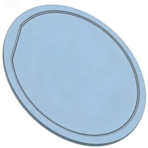
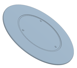
| Used for holding SiC substrates during the growth of SiC epitaxial wafers. Located inside the reaction chamber, in direct contact with the wafer. | A temperature-controlled carrier used to support other components within the SiC epitaxy reactor chamber.Located inside the reaction chamber, not in direct contact with the wafer. |
 |
 |
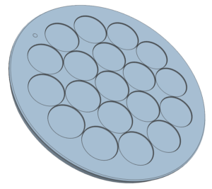
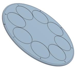
| Holds 19 pieces of 2-inch substrates for the growth of deep ultraviolet (DUV) LED epitaxial wafers. Located inside the reaction chamber, in direct contact with the wafers. | Connects to the quartz tube and enables gas flow to drive rotation of the susceptor base, with controllable temperature. Located inside the reaction chamber, not in direct contact with the wafer. |
 |
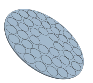 |
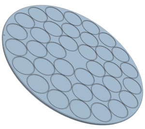
| Holds 34 pieces of 4-inch substrates for the growth of deep ultraviolet (DUV) LED epitaxial wafers. Located inside the reaction chamber, in direct contact with the wafers. | Holds 41 pieces of 4-inch substrates for the growth of deep ultraviolet (DUV) LED epitaxial wafers. Located inside the reaction chamber, in direct contact with the wafers. |
 |
 |
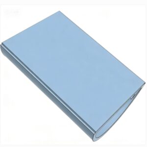
| Holds silicon (Si) substrates for the growth of Si epitaxial wafers, supporting sizes up to 12 inches. Located inside the reaction chamber, in direct contact with the wafer. | Positioned around the outer perimeter of the Si epitaxial susceptor, used for alignment reference and heating, supporting wafer sizes up to 12 inches. Located inside the reaction chamber, not in direct contact with the wafer. |
 |
 |
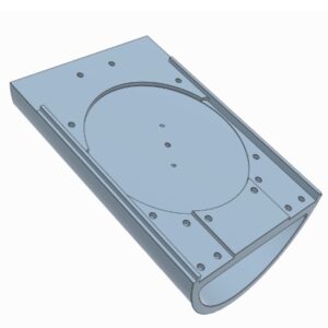
| Multi-Wafer Type – 8 × 6-inch Graphite Base and customized. Holds silicon (Si) substrates for the growth of Si epitaxial wafers. | Customized SiC Epitaxy Equipment and other semiconductor Components. |