
Description
- World class R&D team based at Silicon Valley
- Decades of experience in Semiconductor and Mircoelectronics Industry Metrology
- High Precision
- Easy to Use
- Wide Application
- Best CoO and measurement solution
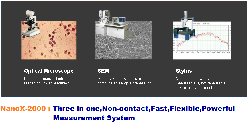
NanoX-2000 is used for measurement and analysis of surface morphology and surface structure of a detection device, can be used for scientific research, but also can be used for the detection of industrial products. Nano x-2000 surface micro topography instrument established in scanning white light interference technology and phase shifting interferometry based, with its high precision and accuracy qualitatively and quantitatively reflects the measured surface roughness, step height, key parts of the size and morphology of etc.. Applicable to the field of semiconductor technology, aerospace, MEMS, ultra precision machining and measurement of super fine surface morphology in nanometer scale.
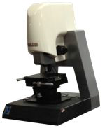
NanoX-2000 3D surface topography measuring apparatus consists of a precision stage, lighting system, optical interference imaging system, realization of phase shifting motion of the micro displacement system, image acquisition system and image data processing system. The detector is placed in the flotation of anti vibration platform. Loading platform for placed the part to be measured, at the same time through the tilt and the two-dimensional XY translational adjustment the measured surface are accurately located in the region of interest; light source and lighting system is provided to the measured surface evenly and fully reflective lighting; interference imaging system using a Mirau interference objective structure is detected to obtain surface interference image; the pressure piezoelectric ceramics (PZT) realize micro displacement control; through the acquisition of CCD and the independent development of software system and processing interference image, to obtain the measured surface phase information and then get the surface profile.
Other Information on NanoX-2000:
Nano x-2000, NanoX-2000, surface morphology , surface structure, detection device, Optical Microscope, SEM, Stylus, Non-contact Measurement, 3D Optical Microscope,Semiconductor,MEMS,LED,IC Packaging,Precision Surface,Solar Cell,Surface Roughness,Surface Coating, Roughness,Step Height,Surface Defects,Film Thickness, Roughness measure,Step Height measure,Surface Defects measure,Film Thickness measure, Roughness measurement,Step Height measurement,Surface Defects measurement,Film Thickness measurement, MEMS Multi-layer structure , Sapphire wafer surface roughness analysis , Sapphire wafer polishing analysis , rough polishing , Silicon wafer backgrinding surface, fine polishing Step height accuracy, Epi layer defect analysis, Epi layer defect,Step height rep, RMS rep,High precision surface defects, MEMS 3D Profile, Precision Machining, LED chip metrology, PI ,nano-stage and control, Nikon,Mirau objectives, NI,DAQ board and Labview64 signal processing, Step Height Standard Comparison,AppNano,PSI,VSI, VSI Mode, PSI Mode,Area roughness, line roughness, defect analysis, scratch depth analysis,Interference, target surface reflection and reference, Interfergrams and Processing,surface micro topography instrument , surface micro topography, white light interference technology , phase shifting interferometry,