Main Maker

Measurement Samples

NanoX-2000  3D surface topography for Semiconductor, MEM, LED,IC Packaging, Precision Surface, Solar Cell, Surface Roughness, Surface Coating etc.

  • MEMS Multi-layer structure
  • Sapphire wafer surface roughness analysis
  • Sapphire wafer polishing analysis via Roughness
  • Silicon wafer backgrinding surface roughness and defect analysis
  • Epi layer defect analysis
Category: Tag:

Description

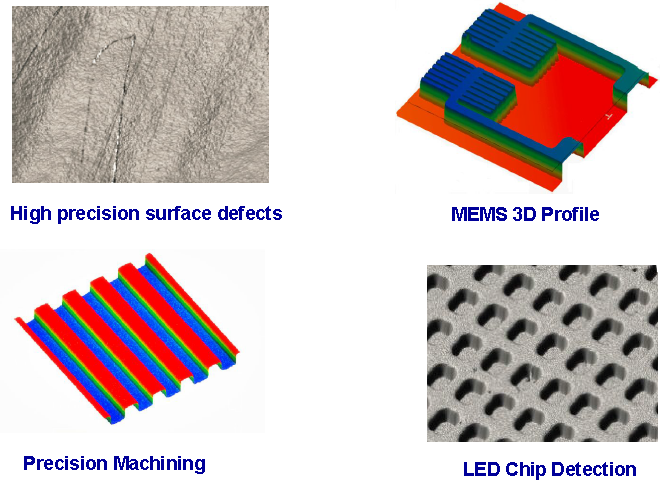
NanoX-2000 – Measurement Samples

NanoX-2000 Measurement Samples

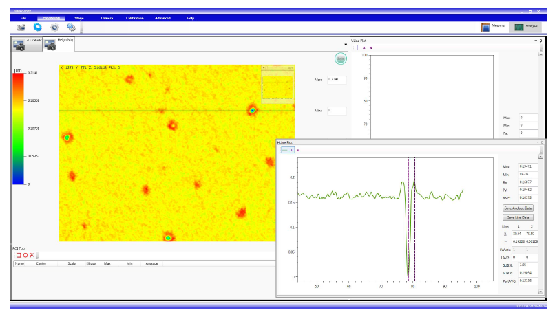
NanoX-2000 – 3D、2D、1D display,data analysis:

NanoX-2000 Measurement Samples-1

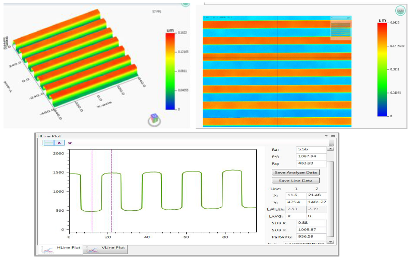
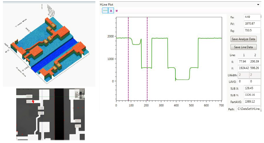
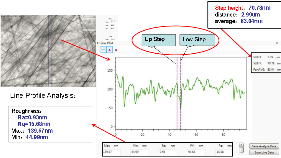
NanoX-2000 – MEMS Multi-layer structure:

NanoX-2000- MEMS Multi-layer structure

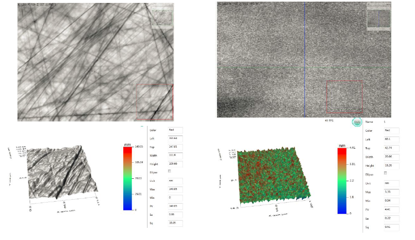
NanoX-2000 – Sapphire wafer surface roughness analysis:

Sapphire wafer surface roughness analysis

NanoX-2000 – Sapphire wafer polishing analysis via Roughness:

Sapphire wafer polishing analysis via Roughness

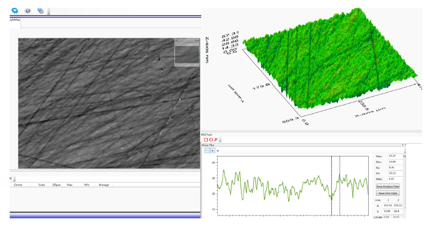
NanoX-2000 – Silicon wafer backgrinding surface roughness and defect analysis:

Silicon wafer backgrinding surface roughness and defect analysis

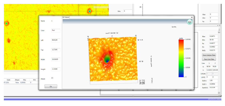
NanoX-2000 – Epi layer defect analysis:

Epi layer defect analysis

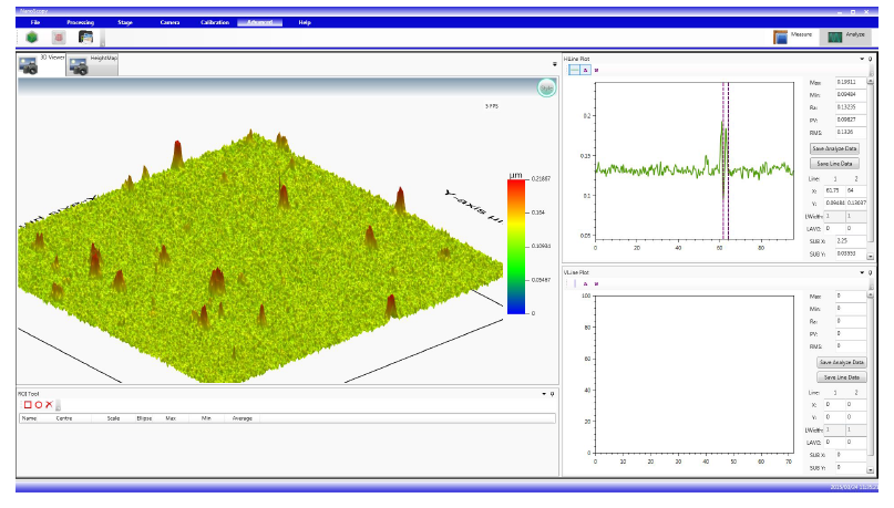
  • Epi layer defect analysis;defect:PV~190nm,radius~2.0um:

Epi layer defect analysis;defect:PV~190nm,radius~2.0um

  • Epi defect analysis,zoom-in 3D view

Epi defect analysis,zoom-in 3D view


Please contact us for more information on the product:

Your Name*:

Your Email:

Your Message:

Captchac Codecaptcha

Submit:

The trademarks of the equipment and parts contained in this website belonged to the Original Equipment Manufacturers