Description
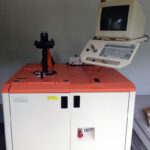
KLA-Tencor Surfscan 6200 (SFS6200):
Wafer Surface Contamination Analysis System
The SFS6200 tool is used for wafer surface contamination analysis of unpatterned semiconductor wafers.
Specifications
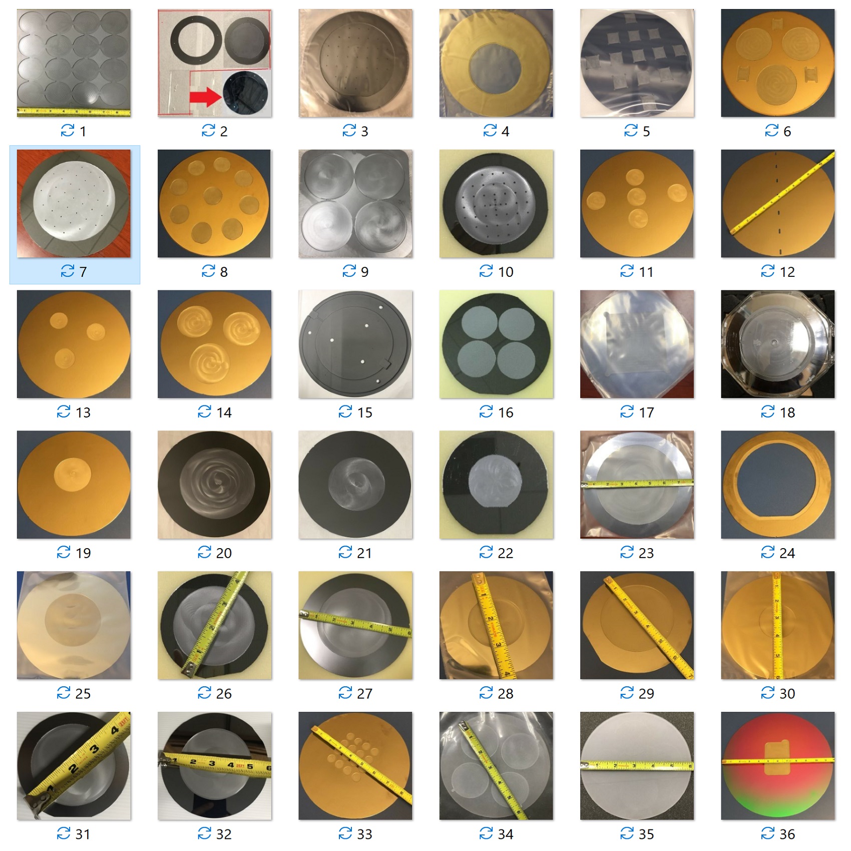
• Substrate Sizes: 50mm(2″), 76mm(3″), 100mm(4″), 125mm(5″), 150mm(6″), 200mm(8″) wafers
• Substrate Material: Silicon or any opaque, polished surface which scatters less than 5% of incident light.
• Defect Sensitivity: 0.10µm diameter PSL sphere equivalent with greater than 90% capture rate.
• Haze Sensitivity: 0.02ppm
• Haze Resolution: 0.002ppm
• Repeatability: 0.5% at 1σ (mean count greater than 500, 0.364 µm diameter latex spheres)
• Accuracy: ≥99% (verified with VLSI Standards)
• Dynamic Range: 0.01µm to 9,999µm in a single measurement.
• Throughput: Up to 100 w/hr using 150mm wafers
• Cassette Handling: Single puck wafer handling from two cassette (one sender/receiver, one receiver)
• Illumination Source: 30mW Argon-Ion laser, 488nm wavelength
• Operator Interface: New LCD monitor, keyboard, mouse
• Color coded defect maps, histograms, magnified views of individual defects.
• Operation System and Software: Windows 98, ver. 4.2
• Manual
Quality Control
• The SFS6200 is calibrated and tested.
Physical Characteristics
• Instrument Dimensions: Height: 168 cm (66”) Width: 75 cm (29.5”) Depth: 77 cm (30.25”)
• Instrument Weight: 240 kg (530 lbs)
• Crate Dimensions: Height 196 cm (77”) Width: 112 cm (44”) Depth: 122 cm (48”)
• Crate Weight: 460 kg (1010 lbs)
Installation Requirements
• Vacuum: 508 mm (20 in.) Hg
• Electrical: 220-240V, 50/60 Hz
• Power Requirement: 2 kVA
• Ducted Venting: Two 102 mm (4”) exhaust hoses
• Environment: Class 10 or better
Condition: Unit pulled from a working service, however due to lack of power supply unable to fully test. Sold As-Is. Complete,working,functional test or refurbished conditions are optional at extra cost.
Valid time: Subject to prior sale without notice. Appreciate your time.
ID-SS380-e