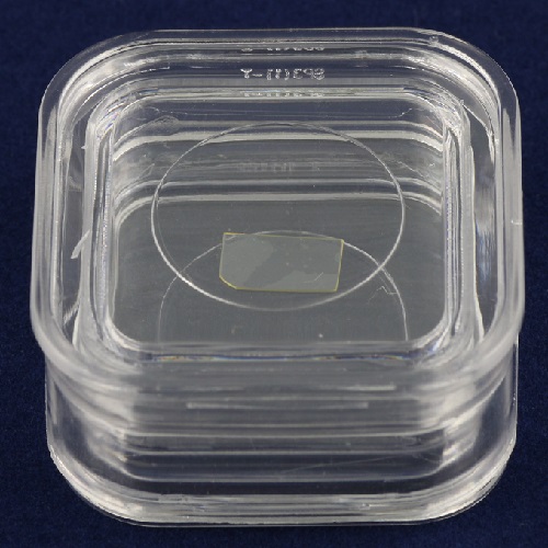
Description
GaSb Wafers- Gallium Antimonide
Note: Surface – P = Polished, E = Etched, C = AsCut, Ox = Oxide (on that surface)
Note: Please email us to check the availability , price and lead time etc.
| Item | Material | Orient. | Diam | Thck | Surf. | Resistivity | Nc | Mobil | EPD | Comment |
| (mm) | (μm) | Ωcm | a/cm3 | cm2/Vs | /cm2 | |||||
| 1 | n-type GaSb:Te | [100-6° towards[111]] ±0.5° | 2″ | 400 | P/E | 0.0019-0.0048 @ 77°K | (4.4-13)E17 @ 77°K | 2,540-2,950 @ 77°K | <10,000 | US Flats; Epi Ready |
| 2 | n-type GaSb:Te | [100] | 2″ | 450 | P/E | 0.0054 | 4.70E+17 | 2,490 | <3,000 | US Flats; Epi Ready |
| 3 | p-type GaSb:Si | [100] | 2″ | 450 | P/E | 0.03 | 2.60E+17 | 780 | <3,000 | US Flats; Epi Ready |
| 4 | p-type GaSb:Si | [100] | 2″ | 450 | P/E | 7.20E-03 | 1.60E+18 | 536 | <2,000 | US Flats; Epi Ready |
| 5 | p-type GaSb:Si | [100] | 2″ | 450 | P/E | 8.20E-04 | 1.60E+19 | 470 | <3,000 | US Flats; Epi Ready |