Description
Perkin-Elmer 4400 Series-4400,4410,4450,4480, Magnetron Sputtering Deposition System Manual in PDF
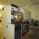
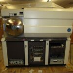
Perkin-Elmer 2400-8L Load Lock Sputtering System
Perkin Elmer Sputtering System 2400 – 8L Load Lock Sputter Deposition Coater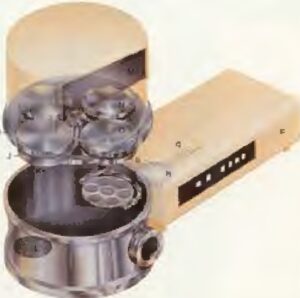
Comes with AE MDX 1K RF Power Generator
Condition: Complete, working, functional test.
Location: Morgan Hill,CA USA
SS-000A-E.D.-MSP-195
Perkin-Elmer,Perkin-Elmer PVD,Perkin-Elmer 半自动磁控溅射,Perkin-Elmer 2400,Perkin-Elmer 2400-8L,Perkin-Elmer 4400,Perkin-Elmer 4410,Perkin-Elmer 4415,Perkin-Elmer 4450,Perkin-Elmer 4480,溅射 PVD,半导体 PVD,半自动溅射机,PVD 薄膜沉积,晶圆涂覆,小批量晶圆,大学研究所 PVD,前道半导体工艺,PVD 工艺优化,PVD 设备维护,PVD 设备翻新,PVD 设备升级,PVD 设备备件,老旧 PVD 翻新,老旧 PVD 支持,PVD 替代备件,晶圆薄膜均匀性,可重复沉积,晶圆表面涂覆,化合物半导体 PVD,GaAs PVD,SiC PVD,InP PVD,GaN PVD,2寸晶圆 PVD,4寸晶圆 PVD,6寸晶圆 PVD,老旧设备支持,PVD 腔体维护,PVD 控制系统维修,PVD 硬件升级,PVD 工艺优化,PVD 温度校准,PVD 气流校准,PVD RF 调整,工艺稳定性,量产 PVD,薄膜工艺重复性,沉积前晶圆清洗,沉积后清洗,PVD 腔体翻新,关键晶圆涂覆,高产能 PVD,低成本 PVD,高可靠性 PVD,SemiStar 库存,SemiStar OEM 备件,SemiStar 工程,SemiStar 全球支持,设备重建服务,精密溅射,薄膜均匀性优化,PVD 沉积速率优化,晶圆表面准备,PVD 工艺配方调整,低损伤 PVD,PVD 自动化改造,PVD 终点控制,晶圆表面保护,PVD 维护,前道半导体 PVD,老旧 PVD 翻新,PVD 升级服务,生产线 PVD 支持,小批量晶圆 PVD,精密晶圆涂覆,PVD 设备恢复,工艺腔体重建,晶圆装载自动化,PVD 工艺校准,沉积前清洗,沉积后剥离,低温 PVD,刻蚀残膜防护,PVD 工具优化,晶圆清洗模块,PVD 腔体清洁,关键清洁工艺,高产 PVD,老化 PVD 改进,老旧 PVD 升级,PVD 硬件恢复,老旧设备维护,精密晶圆清洗,高性能 PVD,老旧设备工程,薄膜沉积解决方案,高均匀性 PVD 工具,高产能 PVD,前道工艺支持,无化学晶圆清洗,老旧系统升级,PVD 腔体翻新,精密晶圆准备,晶圆表面优化,生产线持续支持,PVD 工艺窗口优化,PVD 速率校准,晶圆边缘涂覆,晶圆准备解决方案,高通量晶圆准备,生产线优化,关键晶圆清洁,晶圆准备工具,精密 PVD 调整,老旧系统翻新,PVD 工艺控制,晶圆厂清洗系统,沉积前表面清洗,沉积后表面清洗,PVD 设备服务,SemiStar 翻新,PVD 设备升级,PVD 备件供应,PVD 设备维护,全球 PVD 支持,高可靠 PVD 备件,晶圆涂覆优化,晶圆准备模块,薄膜清洗,薄膜工艺改进,薄膜沉积服务,PVD 工具调试,高通量晶圆准备,晶圆准备服务,PVD 工艺重复性检查,晶圆清洗解决方案,低温晶圆准备,晶圆表面恢复,晶圆准备优化,PVD 工具工程,PVD 腔体调整,PVD 均匀性优化,生产线涂覆支持,高性能晶圆准备,SemiStar OEM 备件,PVD 翻新服务,低损伤晶圆准备,高通量晶圆涂覆,SemiStar 工程支持,老旧 PVD 升级,PVD 翻新方案,晶圆准备优化模块,PVD 工艺稳定性,PVD 清洗方案,晶圆厂涂覆支持,高可靠薄膜,PVD 工艺调试,晶圆清洗模块,精密 PVD 维护,高产晶圆准备,精密涂覆服务,PVD 工具重建,晶圆表面保护,PVD 前道支持,生产线 PVD 服务,高通量 PVD 清洗,PVD 工艺优化服务,老旧 PVD 翻新服务,废弃 PVD 升级,精密晶圆准备方案,Perkin-Elmer,Perkin-Elmer PVD,Perkin-Elmer sputtering,Perkin-Elmer 2400,Perkin-Elmer 2400-8L,Perkin-Elmer 4400,Perkin-Elmer 4410,Perkin-Elmer 4415,Perkin-Elmer 4450,Perkin-Elmer 4480,magnetron sputtering,PVD system,thin film deposition,PVD tool,PVD equipment,semi-automatic sputtering,wafer coating,wafer thin film,small batch PVD,university research lab PVD,Semistar Perkin-Elmer support,Semistar Perkin-Elmer service,Semistar Perkin-Elmer refurbish,Semistar Perkin-Elmer spare parts,refurbished PVD,legacy PVD support,obsolete PVD replacement,thin film uniformity,repeatable deposition,wafer surface coating,compound semiconductor PVD,GaAs PVD,SiC PVD,InP PVD,GaN PVD,2 inch wafer PVD,4 inch wafer PVD,6 inch wafer PVD,aging tool support,PVD chamber maintenance,PVD controller repair,PVD hardware upgrade,PVD process optimization,PVD temperature calibration,PVD gas flow calibration,PVD RF tuning,process stability,production PVD,thin film process repeatability,substrate cleaning before PVD,post-deposition cleaning,PVD chamber refurbish,critical wafer coating,high throughput PVD,low cost PVD,high reliability PVD,SemiStar inventory,SemiStar OEM parts,SemiStar engineering,SemiStar global support,tool rebuild service,precision sputtering,thin film uniformity optimization,PVD rate optimization,wafer surface prep,PVD process recipe tuning,low-damage PVD,PVD automation retrofit,PVD endpoint control,substrate surface protection,PVD maintenance,front-end semiconductor PVD,legacy PVD refurbish,PVD upgrade service,production line PVD support,small batch wafer PVD,precision substrate coating,PVD tool recovery,process chamber rebuild,wafer load automation,PVD process calibration,pre-deposition clean,post-deposition strip,low-temp PVD,etch residue prevention,PVD tool optimization,substrate cleaning module,PVD chamber cleaning,critical clean process,high yield PVD,aging PVD enhancement,old PVD tool upgrade,PVD hardware recovery,obsolete tool maintenance,precision wafer cleaning,high performance PVD,legacy tool engineering,thin film deposition solution,high uniformity PVD tool,high capacity PVD,front-end process support,chemical-free wafer cleaning,legacy system upgrade,PVD chamber refurbish,precision wafer prep,substrate prep optimization,production line continuous support,PVD process window optimization,PVD rate calibration,wafer edge coating,substrate prep solution,high throughput wafer prep,production line optimization,critical wafer clean,substrate prep tool,precision PVD tuning,legacy system refurbish,PVD process control,wafer fab cleaning system,pre-deposition surface clean,post-deposition surface clean,PVD equipment service,SemiStar refurbish,PVD tool upgrade,PVD parts supplier,PVD equipment maintenance,global PVD support,high reliability PVD parts,wafer coating optimization,substrate prep module,thin film clean,thin film process improvement,thin film deposition service,PVD tool tuning,high throughput substrate prep,substrate prep service,PVD process repeatability check,wafer clean solution,low-temp wafer prep,substrate surface restoration,wafer prep optimization,PVD tool engineering,PVD chamber tune,PVD uniformity optimization,production line coating support,high performance wafer prep,SemiStar OEM parts,PVD refurbish service,low damage substrate prep,high throughput wafer coating,SemiStar engineering support,legacy PVD upgrade,PVD refurbish solutions,substrate prep optimization module,PVD process stability,PVD cleaning solution,wafer fab coating support,high reliability thin film,PVD process tuning,substrate clean module,precision PVD maintenance,high yield substrate prep,precision coating service,PVD tool rebuild,wafer surface protection,PVD front-end support,production line PVD service,high throughput PVD cleaning,PVD process optimization service,legacy PVD refurbish service,obsolete PVD tool upgrade,precision wafer prep solution,Physical Vapor Deposition,Magnetron Sputtering,E-beam Evaporation,Thermal Evaporation