Description
- 26″x44″ footprint with enclosed panels ideal for clean rooms
- Fully automatic PC based, recipe driven
- LabVIEW user interface
- EMO protection and safety interlocks
 |
 |
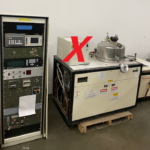
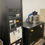
Ion Beam and PVD |
NRP-4000 PECVD and RIE/ ICP/DRIE |
 |
 |
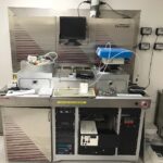
PECVD and Sputtering |
RIE/ICP/DRIE and Sputtering |
 |
|
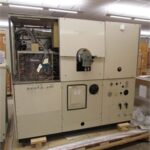
| NLP-4000 PECVD PEALD |
NLE-4000 PAALE PEALD |

NANO-MASTER’S NLP-4000 HYBRID PEALD/PECVD SYSTEM
Due to the chamber design and planar ICP source, both ALD and PECVD processes can be ran within the same NLP-4000 system without the need of mechanical reconfiguration. The hybrid system al-lows for deposition of both thin ALD films and thick PECVD films within the same chamber and process (“recipe”).
HYBRID SYSTEM:
The Nano-Master NLE-4000 series of hybrid system provides both Plasma-Enhanced Atomic Layer Etch-ing (PEALD) and Plasma-Assisted Atomic Layer Etching (PAALE) capability in the same process chamber making it a state-of-the-art ALE tool for Research and Development. Widely used in na-noscale fabrication, MEMS, quantum devices, and advanced semiconductor technologies, our hy-brid PAALE/PEALD system is able to provide damage-free Plasma Assisted Atomic Layer Etching. Nano-Master ALE systems provide soft Atomic Layer Etching using our unique Planar Inductive Coupling Plasma (ICP) source.
NANO-MASTER’S HYBRID PEALD/PAALE SYSTEM ATOMIC LAYER ETCHING:
Atomic Layer Etching (ALE) is a precise material removal technique used in semiconductor manu-facturing that operates at the atomic level. This method ensures ultra-thin layer removal with high fidelity, allowing for selective etching of specific materials while minimizing damage to adja-cent areas. ALE enables precise control over surface morphology, making it essential for advanced device architectures. Characterized by low etch rates, it is ideal for applications requiring meticu-lous layer management typically in the order of monolayers. The process involves alternating cy-cles of surface modification and etching, which enhance uniformity and reproducibility. Addition-ally, ALE is compatible with a variety of materials, including silicon, metals, and dielectrics, and it reduces substrate damage, preserving electrical properties.
The trademarks of the equipment and parts contained on this page belong to the Original Equipment Manufacturers.
Nano-Master Main Equipment: Thin Film | Etch | Cleaning | Space Simulation | Hybrid
SS10840