Description
Please contact us for the availability of the following used Atomic Layer Deposition (ALD) Systems semiconductor equipment
Info from OEM for your reference only.
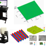
ALD is a thin film deposition process that allows for atomic layer thickness resolution, excellent conformity of high aspect ratio surfaces, and pinhole-free layers. This is achieved by sequential formation of atomic layers in a self-limiting reaction.
ALD is commonly used in the semiconductor industry for high-k dielectric films in CMOS processing, memory devices, MEMS, and sensors. ALD systems are used for development of protective and functional coatings in fuel cells and other applications requiring corrosion or wear resistance. They are also used to coat high aspect ratio structures like nanowires and nanotubes for next generation device development.
Oxides: Al2O3, TiO2, SnO, HfO2, ZnO, Fe2O3
Nitrides: TiN, TaN, WN
Metals: Cu, Ru, Ir, W and more.
The item is only for end user. The item is subject to prior sale without notice.
SS5965