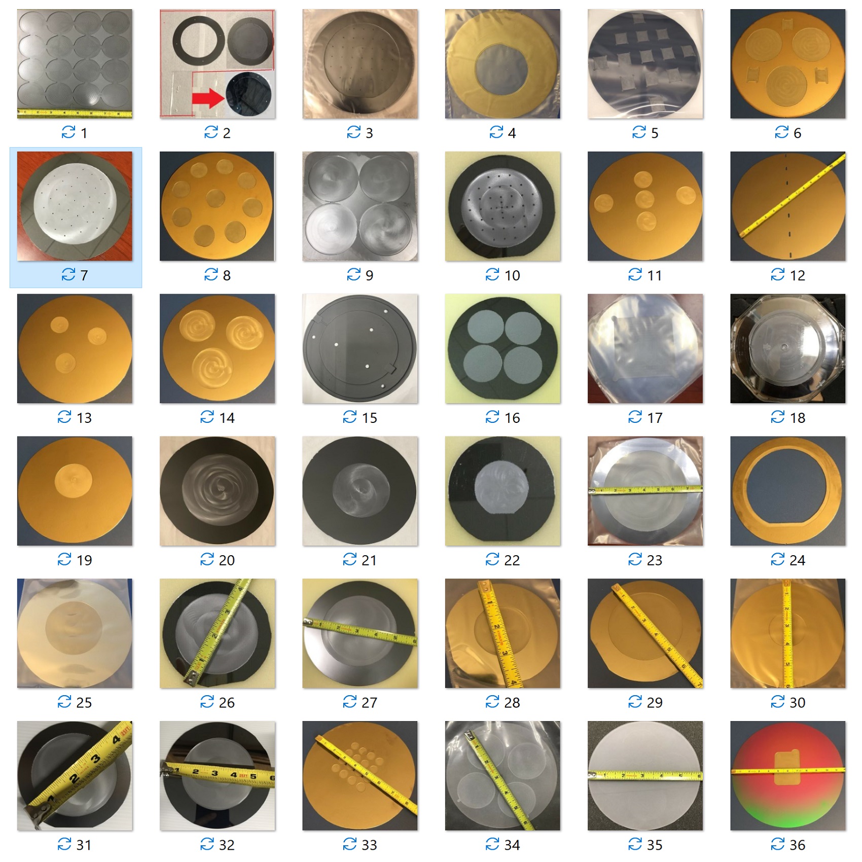
Main Refurbished Equipment for Gallium nitride (GaN) wafers and devices process and metrology measurement.
Gallium nitride (GaN) is a very hard, mechanically stable, binary III/V direct bandgap semiconductor. With higher breakdown strength, faster switching speed, higher thermal conductivity and lower on-resistance, power devices based on GaN significantly outperform silicon-based devices.Since the 1990s, it has been used commonly in light emitting diodes (LED). Gallium nitride gives off a blue light used for disc-reading in Blu-ray. Additionally, gallium nitride is used in semiconductor power devices, RF components, lasers, and photonics. In the future, we will see GaN in sensor technology.Bulk GaN is non-toxic and biocompatible. Therefore, it may be used in the electrodes and electronics of implants in living organisms.
Gallium nitride, or GaN, has a higher breakdown voltage, which allows it to handle higher voltages than silicon to experience an electrical breakdown. This means GaN-based devices can operate at higher power levels without compromising performance.Gallium nitride (GaN) is a binary III/V direct bandgap semiconductor commonly used in blue light-emitting diodes since the 1990s. The compound is a very hard material that has a Wurtzite crystal structure. Its wide band gap of 3.4 eV affords it special properties for applications in optoelectronic, high-power and high-frequency devices. For example, GaN is the substrate that makes violet (405 nm) laser diodes possible, without requiring nonlinear optical frequency doubling.Its sensitivity to ionizing radiation is low (like other group III nitrides), making it a suitable material for solar cell arrays for satellites. Military and space applications could also benefit as devices have shown stability in high radiation environments.GaN dust is an irritant to skin, eyes and lungs. The environment, health and safety aspects of gallium nitride sources (such as trimethylgallium and ammonia) and industrial hygiene monitoring studies of MOVPE sources have been reported in a 2004 review.Schottky diode.Semiconductor devices.Molecular-beam epitaxy.Epitaxy.Lithium-ion battery.Bulk GaN is non-toxic and biocompatible. Therefore, it may be used in the electrodes and electronics of implants in living organisms.
In nature, gallium occurs only to a small extent and mostly as an admixture in aluminum, zinc or germanium ores; Gallium minerals are very rare. Accordingly, it is also obtained as a by-product in the production of aluminum or zinc.The unique properties of GaN, such as its lattice mismatch with commonly used substrates, require developing novel manufacturing methods to ensure high-quality device production. Researchers are currently working on more sustainable manufacturing methods.Light-emitting diodes (LEDs) fabricated from gallium nitride (GaN) have led to the realization of high-efficiency white solid-state lighting. Currently, GaN white LEDs exhibit luminous efficacy greater than 150 lm W−1, and external quantum efficiencies higher than 60%.Because GaN transistors can operate at much higher temperatures and work at much higher voltages than gallium arsenide (GaAs) transistors, they make ideal power amplifiers at microwave frequencies. In addition, GaN offers promising characteristics for THz devices. Due to high power density and voltage breakdown limits GaN is also emerging as a promising candidate for 5G cellular base station applications. Since the early 2020s, GaN power transistors have come into increasing use in power supplies in electronic equipment, converting AC mains electricity to low-voltage DC.Global lithium supplies may be dwindling, but we can still cut energy costs by using less lithium and opting for another material instead. Electric vehicle systems usually use silicon semiconductors, but they’re not the only option. Gallium nitride, for instance, offers higher energy density and saves on weight.
Pros of GaN Chargers :High Efficiency. GaN Chargers can convert and transfer more power from the wall plug to the device ,making them more efficient and productive.Compact Size.Faster Charging Speed.Reduce Generated Heat.Durability and Robustness. Higher Cost.Compatibility Issue.Availability.GaN HEMTs, which use a lateral-type structure where the current flow is horizontal, have limitations in high-power applications where the high voltages and currents involved would require such a large die area that it would be difficult to manufacture.Gallium is a CORROSIVE CHEMICAL and contact can severely irritate and burn the skin and eyes with possible eye damage. * Breathing Gallium can irritate the nose and throat causing coughing and wheezing. * Gallium may damage the liver and kidneys. * Gallium may affect the nervous system and lungs.GaN is a very hard (Knoop hardness 14.21 GPa: 4 ), mechanically stable wide-bandgap semiconductor material with high heat capacity and thermal conductivity. In its pure form it resists cracking and can be deposited in thin film on sapphire or silicon carbide, despite the mismatch in their lattice constants. GaN can be doped with silicon (Si) or with oxygen to n-type and with magnesium (Mg) to p-type. However, the Si and Mg atoms change the way the GaN crystals grow, introducing tensile stresses and making them brittle. Gallium nitride compounds also tend to have a high dislocation density, on the order of 108 to 1010 defects per square centimeter.Gallium is known for its ability to weaken or “liquid metal embrittlement” (LME) in certain metals. The metals that are particularly susceptible to gallium-induced weakening include aluminum, indium, tin, and zinc.
No one was able to grow gallium nitride crystals of high enough quality, since it was seen as a hopeless endeavour to try to produce a fitting surface to grow the gallium nitride crystal on. Moreover, it was virtually impossible to create p-type layers in this material.Gallium Nitride Technology: A Revolution in Semiconductors.GaN’s ability to conduct electrons more than 1000 times more efficiently than silicon, while being able to be manufactured at a lower cost than silicon has now been well established.he U.S. Army Research Laboratory (ARL) provided the first measurement of the high field electron velocity in GaN in 1999. Scientists at ARL experimentally obtained a peak steady-state velocity of 1.9×107 cm/s, with a transit time of 2.5 picoseconds, attained at an electric field of 225 kV/cm. With this information, the electron mobility was calculated, thus providing data for the design of GaN devices.
China accounts for 95 percent of the global supply of soft, bluish metal.SiC typically has better thermal resistivity than both GaN and silicon, and as such, yields a higher number of chips per wafer.Gallium nitride (GaN) was synthesized by Juza and Hahn (1940) who passed ammonia over hot gallium.One of the earliest synthesis of gallium nitride was at the George Herbert Jones Laboratory in 1932.An early synthesis of gallium nitride was by Robert Juza and Harry Hahn in 1938.GaN with a high crystalline quality can be obtained by depositing a buffer layer at low temperatures. Such high-quality GaN led to the discovery of p-type GaN, p–n junction blue/UV-LEDs and room-temperature stimulated emission (essential for laser action). This has led to the commercialization of high-performance blue LEDs and long-lifetime violet laser diodes, and to the development of nitride-based devices such as UV detectors and high-speed field-effect transistors.Although an LED lamp holds a relatively small amount of gallium (about 0.025g per LED) and other metals, the increasing value of these metals means that a solution that maximises volume while minimising costs could be quite profitable.
Gallium nitride (GaN) is a well-known non-magnetic semiconductor material. However it can be transformed into magnetic material, i.e. diluted magnetic semiconductor (DMS), by adding magnetic materials as impurities.Gallium nitride is biocompatible and non-toxic before and after functionalization with peptides.The main downside of GaN chargers lies in their cost. The sophisticated synthesis and manufacturing process of GaN materials results in relatively high prices for GaN chargers. This can limit their widespread adoption in the mid-to-low-end market, making them less appealing to budget-conscious consumers.High-brightness GaN light-emitting diodes (LEDs) completed the range of primary colors, and made possible applications such as daylight-visible full-color LED displays, white LEDs and blue laser devices. The first GaN-based high-brightness LEDs used a thin film of GaN deposited via metalorganic vapour-phase epitaxy (MOVPE) on sapphire. Other substrates used are zinc oxide, with lattice constant mismatch of only 2% and silicon carbide (SiC). Group III nitride semiconductors are, in general, recognized as one of the most promising semiconductor families for fabricating optical devices in the visible short-wavelength and UV region.
Silver and gallium form an alloy Ag2Ga via a room temperature spontaneous self-assembly that exhibits remarkable mechanical and electrical properties suitable for nanoscale measurementsThe very high breakdown voltages, high electron mobility, and high saturation velocity of GaN has made it an ideal candidate for high-power and high-temperature microwave applications, as evidenced by its high Johnson’s figure of merit. Potential markets for high-power/high-frequency devices based on GaN include microwave radio-frequency power amplifiers (e.g., those used in high-speed wireless data transmission) and high-voltage switching devices for power grids. A potential mass-market application for GaN-based RF transistors is as the microwave source for microwave ovens, replacing the magnetrons currently used. The large band gap means that the performance of GaN transistors is maintained up to higher temperatures (~400 °C) than silicon transistors (~150 °C) because it lessens the effects of thermal generation of charge carriers that are inherent to any semiconductor. The first gallium nitride metal semiconductor field-effect transistors (GaN MESFET) were experimentally demonstrated in 1993 and they are being actively developed.
It was established that at a temperature of 843-893~ a reaction takes place between titanium and gallium, with the formation of the intermetallic compounds Ti3Ga and Ti2Ga. The thermal effect of the formation of Ti3Ga was found to be equal to 10.5 • 0.5 kcal/mole.In 2010, the first enhancement-mode GaN transistors became generally available. Only n-channel transistors were available. These devices were designed to replace power MOSFETs in applications where switching speed or power conversion efficiency is critical. These transistors are built by growing a thin layer of GaN on top of a standard silicon wafer, often referred to as GaN-on-Si by manufacturers. This allows the FETs to maintain costs similar to silicon power MOSFETs but with the superior electrical performance of GaN. Another seemingly viable solution for realizing enhancement-mode GaN-channel HFETs is to employ a lattice-matched quaternary AlInGaN layer of acceptably low spontaneous polarization mismatch to GaN.GaN power ICs monolithically integrate a GaN FET, GaN-based drive circuitry and circuit protection into a single surface-mount device. Integration means that the gate-drive loop has essentially zero impedance, which further improves efficiency by virtually eliminating FET turn-off losses. Academic studies into creating low-voltage GaN power ICs began at the Hong Kong University of Science and Technology (HKUST) and the first devices were demonstrated in 2015. Commercial GaN power IC production began in 2018.In 2016 the first GaN CMOS logic using PMOS and NMOS transistors was reported with gate lengths of 0.5 μm (gate widths of the PMOS and NMOS transistors were 500 μm and 50 μm, respectively).GaN-based violet laser diodes are used to read Blu-ray Discs. The mixture of GaN with In (InGaN) or Al (AlGaN) with a band gap dependent on the ratio of In or Al to GaN allows the manufacture of light-emitting diodes (LEDs) with colors that can go from red to ultra-violet.
GaN transistors are suitable for high frequency, high voltage, high temperature and high-efficiency applications. GaN is efficient at transferring current, and this ultimately means that less energy is lost to heat. GaN high-electron-mobility transistors (HEMT) have been offered commercially since 2006, and have found immediate use in various wireless infrastructure applications due to their high efficiency and high voltage operation. A second generation of devices with shorter gate lengths will address higher-frequency telecom and aerospace applications.GaN-based metal–oxide–semiconductor field-effect transistors (MOSFET) and metal–semiconductor field-effect transistor (MESFET) transistors also offer advantages including lower loss in high power electronics, especially in automotive and electric car applications.Since 2008 these can be formed on a silicon substrate. High-voltage (800 V) Schottky barrier diodes (SBDs) have also been made.The higher efficiency and high power density of integrated GaN power ICs allows them to reduce the size, weight and component count of applications including mobile and laptop chargers, consumer electronics, computing equipment and electric vehicles.GaN-based electronics (not pure GaN) have the potential to drastically cut energy consumption, not only in consumer applications but even for power transmission utilities.Unlike silicon transistors that switch off due to power surges, GaN transistors are typically depletion mode devices (i.e. on / resistive when the gate-source voltage is zero). Several methods have been proposed to reach normally-off (or E-mode) operation, which is necessary for use in power electronics:the implantation of fluorine ions under the gate (the negative charge of the F-ions favors the depletion of the channel)the use of a MIS-type gate stack, with recess of the AlGaN the integration of a cascaded pair constituted by a normally-on GaN transistor and a low voltage silicon MOSFET the use of a p-type layer on top of the AlGaN/GaN heterojunction.
Moreover, it is also difficult to produce GaN substrates on which GaN crystals can be grown. Together, these issues with GaN make mass production complicated and expensive compared to silicon. Consideration should be given to how concentrated R&D efforts can gradually overcome these issues.GaN technology is also utilized in military electronics such as active electronically scanned array radars.Thales Group introduced the Ground Master 400 radar in 2010 utilizing GaN technology. In 2021 Thales put in operation more than 50,000 GaN Transmitters on radar systems.The U.S. Army funded Lockheed Martin to incorporate GaN active-device technology into the AN/TPQ-53 radar system to replace two medium-range radar systems, the AN/TPQ-36 and the AN/TPQ-37.The AN/TPQ-53 radar system was designed to detect, classify, track, and locate enemy indirect fire systems, as well as unmanned aerial systems.The AN/TPQ-53 radar system provided enhanced performance, greater mobility, increased reliability and supportability, lower life-cycle cost, and reduced crew size compared to the AN/TPQ-36 and the AN/TPQ-37 systems. Lockheed Martin fielded other tactical operational radars with GaN technology in 2018, including TPS-77 Multi Role Radar System deployed to Latvia and Romania.In 2019, Lockheed Martin’s partner ELTA Systems Limited, developed a GaN-based ELM-2084 Multi Mission Radar that was able to detect and track air craft and ballistic targets, while providing fire control guidance for missile interception or air defense artillery.On April 8, 2020, Saab flight tested its new GaN designed AESA X-band radar in a JAS-39 Gripen fighter. Saab already offers products with GaN based radars, like the Giraffe radar, Erieye, GlobalEye, and Arexis EW. Saab also delivers major subsystems, assemblies and software for the AN/TPS-80 (G/ATOR).
Bulk GaN is non-toxic and biocompatible. Therefore, it may be used in the electrodes and electronics of implants in living organisms.GaN nanotubes and nanowires are proposed for applications in nanoscale electronics, optoelectronics and biochemical-sensing applications.When doped with a suitable transition metal such as manganese, GaN is a promising spintronics material (magnetic semiconductors).GaN crystals can be grown from a molten Na/Ga melt held under 100 atmospheres of pressure of N2 at 750 °C. As Ga will not react with N2 below 1000 °C, the powder must be made from something more reactive, usually in one of the following ways:2 Ga + 2 NH3 → 2 GaN + 3 H2 or Ga2O3 + 2 NH3 → 2 GaN + 3 H2O. Gallium nitride can also be synthesized by injecting ammonia gas into molten gallium at 900–980 °C at normal atmospheric pressure.Blue, white and ultraviolet LEDs are grown on industrial scale by MOVPE. The precursors are ammonia with either trimethylgallium or triethylgallium, the carrier gas being nitrogen or hydrogen. Growth temperature ranges between 800 and 1100 °C. Introduction of trimethylaluminium and/or trimethylindium is necessary for growing quantum wells and other kinds of heterostructures.Commercially, GaN crystals can be grown using molecular beam epitaxy or metalorganic vapour phase epitaxy. This process can be further modified to reduce dislocation densities. First, an ion beam is applied to the growth surface in order to create nanoscale roughness. Then, the surface is polished. This process takes place in a vacuum. Polishing methods typically employ a liquid electrolyte and UV irradiation to enable mechanical removal of a thin oxide layer from the wafer. More recent methods have been developed that utilize solid-state polymer electrolytes that are solvent-free and require no radiation before polishing.And since it stays cooler, charging speed consistency is maintained. For instance, a multi-port 100-watt and greater capacity chargers have become relevant for phones, tablets and laptops. The flipside, GaN technology is still relatively new, and you do pay a slight premium for these chargers.
Global lithium supplies may be dwindling, but we can still cut energy costs by using less lithium and opting for another material instead. Electric vehicle systems usually use silicon semiconductors, but they’re not the only option. Gallium nitride, for instance, offers higher energy density and saves on weight.The global gallium nitride semiconductor devices market size was estimated at USD 2.56 billion in 2023 and is projected to grow at a CAGR of 26.4% from 2024 to 2030.Blue light has a higher energy compared to red and green light, requiring specific semiconductor materials with wider energy bandgaps to emit blue photons. Developing such materials with the required properties was a significant scientific and engineering challenge.Together with Isamu Akasaki and Hiroshi Amano, Nakamura received the 2014 Nobel Prize for Physics “for the invention of efficient blue light-emitting diodes, which has enabled bright and energy-saving white light sources”.Each color requires a different voltage. Shorter wavelength photons are more energetic, so blue LEDs typically require a higher voltage than red LEDs to turn on. This is also known as the “forward voltage drop” of the LED. Different colors require different amounts of current to produce the same brightness.Light-emitting diodes (LEDs) fabricated from gallium nitride (GaN) have led to the realization of high-efficiency white solid-state lighting. Currently, GaN white LEDs exhibit luminous efficacy greater than 150 lm W−1, and external quantum efficiencies higher than 60%.Gallium is a main component in many LED lights, with different gallium compounds producing different colored light when exposed to an electric current. LED lights are commonly used in television screens, flashlights, and Christmas lights.
In nature, gallium occurs only to a small extent and mostly as an admixture in aluminum, zinc or germanium ores; Gallium minerals are very rare. Accordingly, it is also obtained as a by-product in the production of aluminum or zinc.The unique properties of GaN, such as its lattice mismatch with commonly used substrates, require developing novel manufacturing methods to ensure high-quality device production. Researchers are currently working on more sustainable manufacturing methods.Apple could release a new 30W charger this year that uses gallium nitride (GaN) in its construction, according to Apple analyst Ming-Chi Kuo. Gallium nitride is a material that allows chargers to produce less heat, which means they can be smaller while still offering high wattages.Unlike silicon chargers, GaN USB-C chargers use semiconductors made from Gallium Nitride to convert AC power from a socket into DC power that is safe for a device. Most are USB-C wall chargers that plug in directly and have universal USB-C ports for the power delivery out.If you’re looking for a fast charger for your iPhone 15, opt for a GaN charger. Gallium Nitride chargers outperform traditional silicon-based chargers in terms of their higher electron mobility, faster charging times, reduced energy losses, compacter sizes, and versatile compatibility.
Main Refurbished Equipment for Gallium nitride (GaN) wafers and devices process and metrology measurement.
The info on this page are from wikipedia and internet. All the rights belong to the original writer.