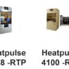
AG Associates Heatpulse 4100 specifications AG Associates Heatpulse 8108 specifications AG Associates Heatpulse 8800 specifications AG Associates Heatpulse 8800i specifications AG Associates Quartz Liner Option and Retrofit Kit Enhanced Z-axis Direct Thermocouple Control (ez-DTC) For Heatpulse® 8800 and 8108 Systems De-ionized Water Retrofit Kit For Heatpulse® Oven Cooling Systems Ceramic Shield Option and Retrofit Kit […]
Archive | Uncategorized
Buying and Selling Used Semiconductor Equipment Business Overview
The global Buying and Selling Used Semiconductor Equipment market size was US$ 3612 million in 2024 and is forecast to a readjusted size of US$ 9661 million by 2031 with a CAGR of 15.3% during the forecast period 2025-2031.The following manufacturers are the key players. SemiStar Corp. ASML KLA Pro Systems Lam Research ASM International […]
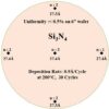
Deposition of Si3N4,ALD SAMPLE DATA
Atomic layer deposition (ALD) is an important technique for depositing thin films for a variety of applications. ALD provides precise thickness control and conformal deposition for high aspect ra-tio applications, exceeding the level of other deposition methods. The sequential, self-limiting surface reactions in ALD produce a non-statistical deposition as precursor flux randomness is a non-factor. […]
Gallium arsenide (GaAs)
Main Refurbished Equipment for Gallium arsenide (GaAs) wafer and devices process and metrology measurement. GaAs is often used as a substrate material for the epitaxial growth of other III-V semiconductors, including indium gallium arsenide, aluminum gallium arsenide and others. The impurities used may be phosphorus, arsenic, antimony, bismuth, or some other chemical element. EXPLANATION: From […]
Silicon carbide (SiC)
Main Refurbished Equipment for Silicon carbide (SiC) wafers and devices process equipment and metrology measurement. Silicon carbide (SiC) is a compound of silicon and carbon with a chemical formula of SiC. The simplest manufacturing process for producing silicon carbide is to combine silica sand and carbon in an Acheson graphite electric resistance furnace at a […]
Indium phosphide (InP)
Main Refurbished Equipment for Indium phosphide (InP) wafer and devices process and metrology measurement. Indium is used to dope germanium to make transistors. It is also used to make other electrical components such as rectifiers, thermistors and photoconductors. Indium can be used to make mirrors that are as reflective as silver mirrors but do not […]
Gallium nitride (GaN)
Main Refurbished Equipment for Gallium nitride (GaN) wafers and devices process and metrology measurement. Gallium nitride (GaN) is a very hard, mechanically stable, binary III/V direct bandgap semiconductor. With higher breakdown strength, faster switching speed, higher thermal conductivity and lower on-resistance, power devices based on GaN significantly outperform silicon-based devices.Since the 1990s, it has been […]
Indium gallium phosphide (InGaP)
Main Refurbished Equipment for Indium gallium phosphide (InGaP) wafers and devices process and metrology measurement . Indium gallium phosphide (InGaP), also called gallium indium phosphide (GaInP), is a semiconductor composed of indium, gallium and phosphorus. It is used in high-power and high-frequency electronics because of its superior electron velocity with respect to the more common semiconductors […]
Semiconductor fabrication
Main Refurbished Equipment for Semiconductor device fabrication. Semiconductor device fabrication is the process used to manufacture semiconductor devices, typically integrated circuits (ICs) such as computer processors, microcontrollers, and memory chips (such as NAND flash and DRAM). It is a multiple-step photolithographic and physico-chemical process (with steps such as thermal oxidation, thin-film deposition, ion-implantation, etching) during […]
Alcatel A601E ICP-DRIE
Alcatel A601E ICP-DRIE