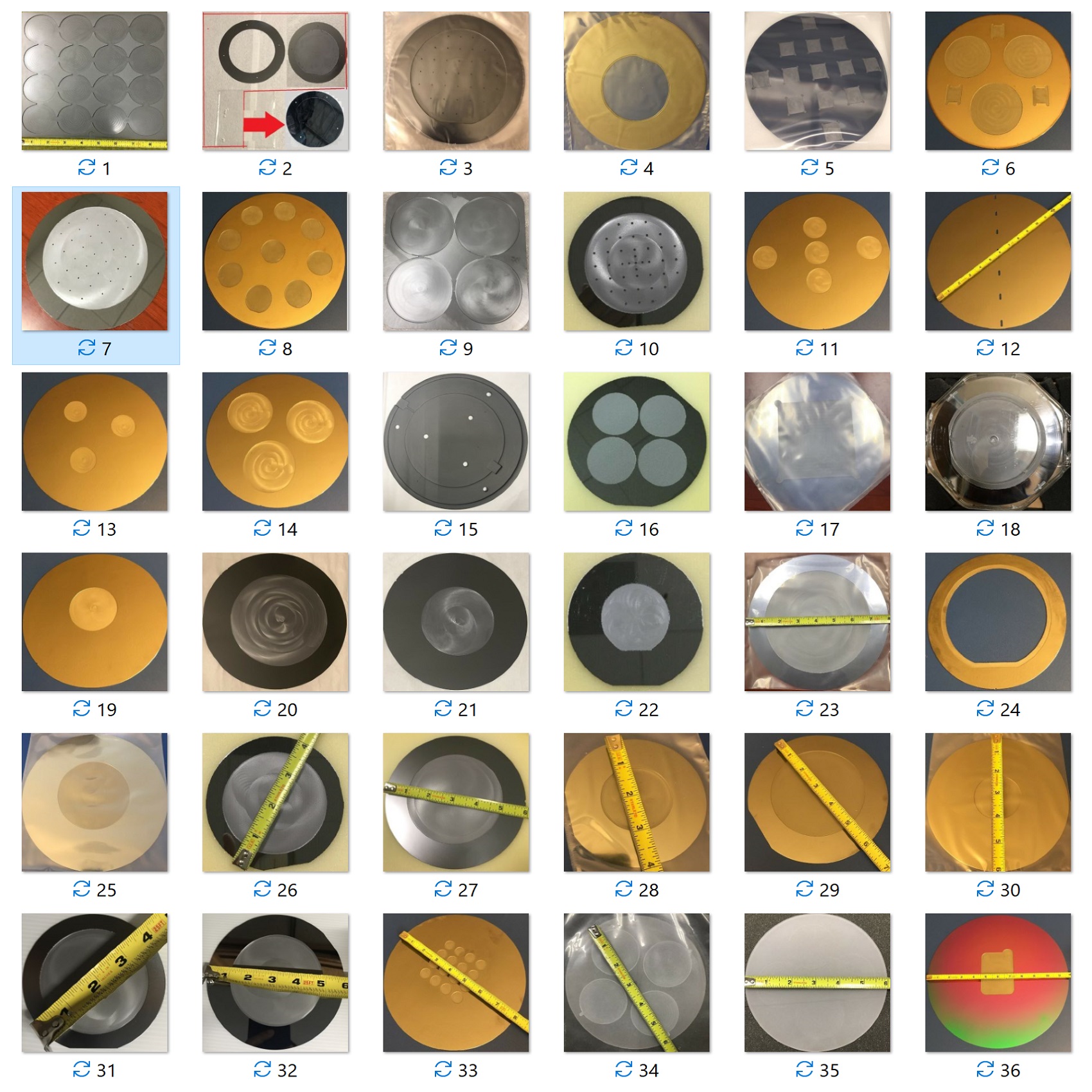
Main Refurbished Equipment for Indium gallium phosphide (InGaP) wafers and devices process and metrology measurement .
Indium gallium phosphide (InGaP), also called gallium indium phosphide (GaInP), is a semiconductor composed of indium, gallium and phosphorus. It is used in high-power and high-frequency electronics because of its superior electron velocity with respect to the more common semiconductors silicon and gallium arsenide.It is used mainly in HEMT and HBT structures, but also for the fabrication of high efficiency solar cells used for space applications and, in combination with aluminium (AlGaInP alloy) to make high brightness LEDs with orange-red, orange, yellow, and green colors. Some semiconductor devices such as EFluor Nanocrystal use InGaP as their core particle.Indium gallium phosphide is a solid solution of indium phosphide and gallium phosphide.Ga0.5In0.5P is a solid solution of special importance, which is almost lattice matched to GaAs. This allows, in combination with (AlxGa1−x)0.5In0.5, the growth of lattice matched quantum wells for red emitting semiconductor lasers, e.g., red emitting (650nm) RCLEDs or VCSELs for PMMA plastic optical fibers.Ga0.5In0.5P is used as the high energy junction on double and triple junction photovoltaic cells grown on GaAs. Recent years have shown GaInP/GaAs tandem solar cells with AM0 (sunlight incidence in space = 1.35 kW/m2) ficiencies in excess of 25%.A different composition of GaInP, lattice matched to the underlying GaInAs, is utilized as the high energy junction GaInP/GaInAs/Ge triple junction photovoltaic cells.Growth of GaInP by epitaxy can be complicated by the tendency of GaInP to grow as an ordered material, rather than a truly random solid solution (i.e., a mixture). This changes the bandgap and the electronic and optical properties of the material.
Gallium phosphide ,Indium(III) phosphide,Indium gallium nitride,Indium gallium arsenide,GaInP/GaAs solar cell.
Gallium phosphide (GaP), a phosphide of gallium, is a compound semiconductor material with an indirect band gap of 2.24 eV at room temperature. Impure polycrystalline material has the appearance of pale orange or grayish pieces. Undoped single crystals are orange, but strongly doped wafers appear darker due to free-carrier absorption. It is odorless and insoluble in water.GaP has a microhardness of 9450 N/mm2, a Debye temperature of 446 K (173 °C), and a thermal expansion coefficient of 5.3 ×10⁻⁶ K−1 at room temperature. Sulfur, silicon or tellurium are used as dopants to produce n-type semiconductors. Zinc is used as a dopant for the p-type semiconductor.Gallium phosphide has applications in optical systems.Its static dielectric constant is 11.1 at room temperature.Its refractive index varies between ~3.2 and 5.0 across the visible range, which is higher than in most other semiconducting materials. In its transparent range, its index is higher than almost any other transparent material, including gemstones such as diamond, or non-oxide lenses such as zinc sulfide.Gallium phosphide has been used in the manufacture of low-cost red, orange, and green light-emitting diodes (LEDs) with low to medium brightness since the 1960s. It is used standalone or together with gallium arsenide phosphide.Pure GaP LEDs emit green light at a wavelength of 555 nm. Nitrogen-doped GaP emits yellow-green (565 nm) light, zinc oxide doped GaP emits red (700 nm).Gallium phosphide is transparent for yellow and red light, therefore GaAsP-on-GaP LEDs are more efficient than GaAsP-on-GaAs.At temperatures above ~900 °C, gallium phosphide dissociates and the phosphorus escapes as a gas. In crystal growth from a 1500 °C melt (for LED wafers), this must be prevented by holding the phosphorus in with a blanket of molten boric oxide in inert gas pressure of 10–100 atmospheres. The process is called liquid encapsulated Czochralski (LEC) growth, an elaboration of the Czochralski process used for silicon wafers.
Indium phosphide (InP) is a binary semiconductor composed of indium and phosphorus. It has a face-centered cubic (“zincblende”) crystal structure, identical to that of GaAs and most of the III-V semiconductors.Indium phosphide can be prepared from the reaction of white phosphorus and indium iodide at 400 °C., also by direct combination of the purified elements at high temperature and pressure, or by thermal decomposition of a mixture of a trialkyl indium compound and phosphine.The application fields of InP splits up into three main areas. It is used as the basis for optoelectronic components,high-speed electronics,and photovoltaics InP is used as a substrate for epitaxial optoelectronic devices based other semiconductors, such as indium gallium arsenide. The devices include pseudomorphic heterojunction bipolar transistors that could operate at 604 GHz.InP itself has a direct bandgap, making it useful for optoelectronics devices like laser diodes and photonic integrated circuits for the optical telecommunications industry, to enable wavelength-division multiplexing applications.It is used in high-power and high-frequency electronics because of its superior electron velocity with respect to the more common semiconductors silicon and gallium arsenide.InP is used in lasers, sensitive photodetectors and modulators in the wavelength window typically used for telecommunications, i.e., 1550 nm wavelengths, as it is a direct bandgap III-V compound semiconductor material. The wavelength between about 1510 nm and 1600 nm has the lowest attenuation available on optical fibre (about 0.2 dB/km). Further, O-band and C-band wavelengths supported by InP facilitate single-mode operation, reducing effects of intermodal dispersion.InP can be used in photonic integrated circuits that can generate, amplify, control and detect laser light.Optical sensing applications of InP include Air pollution control by real-time detection of gases (CO, CO2, NOX [or NO + NO2], etc.).,quick verification of traces of toxic substances in gases and liquids, including tap water, or surface contaminations,Spectroscopy for non-destructive control of product, such as food. Researchers of Eindhoven University of Technology and MantiSpectra have already demonstrated the application of an integrated near-infrared spectral sensor for milk. In addition, it has been proven that this technology can also be applied to plastics and illicit drugs.
Indium gallium nitride (InGaN, InxGa1−xN) is a semiconductor material made of a mix of gallium nitride (GaN) and indium nitride (InN). It is a ternary group III/group V direct bandgap semiconductor. Its bandgap can be tuned by varying the amount of indium in the alloy. InxGa1−xN has a direct bandgap span from the infrared (0.69 eV) for InN to the ultraviolet (3.4 eV) of GaN. The ratio of In/Ga is usually between 0.02/0.98 and 0.3/0.7.Indium gallium nitride is the light-emitting layer in modern blue and green LEDs and often grown on a GaN buffer on a transparent substrate as, e.g. sapphire or silicon carbide. It has a high heat capacity and its sensitivity to ionizing radiation is low (like other group III nitrides), making it also a potentially suitable material for solar photovoltaic devices, specifically for arrays for satellites.It is theoretically predicted that spinodal decomposition of indium nitride should occur for compositions between 15% and 85%, leading to In-rich and Ga-rich InGaN regions or clusters. However, only a weak phase segregation has been observed in experimental local structure studies. Other experimental results using cathodoluminescence and photoluminescence excitation on low In-content InGaN multi-quantum wells have demonstrated that providing correct material parameters of the InGaN/GaN alloys, theoretical approaches for AlGaN/GaN systems also apply to InGaN nanostructures.GaN is a defect-rich material with typical dislocation densities exceeding 108 cm−2. Light emission from InGaN layers grown on such GaN buffers used in blue and green LEDs is expected to be attenuated because of non-radiative recombination at such defects. Nevertheless, InGaN quantum wells, are efficient light emitters in green, blue, white and ultraviolet light-emitting diodes and diode lasers. The indium-rich regions have a lower bandgap than the surrounding material and create regions of reduced potential energy for charge carriers. Electron-hole pairs are trapped there and recombine with emission of light, instead of diffusing to crystal defects where the recombination is non-radiative. Also, self-consistent computer simulations have shown that radiative recombination is focused where regions are rich of indium.The emitted wavelength, dependent on the material’s band gap, can be controlled by the GaN/InN ratio, from near ultraviolet for 0.02In/0.98Ga through 390 nm for 0.1In/0.9Ga, violet-blue 420 nm for 0.2In/0.8Ga, to blue 440 nm for 0.3In/0.7Ga, to red for higher ratios and also by the thickness of the InGaN layers which are typically in the range of 2–3 nm. However, atomistic simulations results have shown that emission energies have a minor dependence on small variations of device dimensions. Studies based on device simulation have shown that it could be possible to increase InGaN/GaN LED efficiency using band gap engineering, especially for green LEDs.The ability to perform bandgap engineering with InGaN over a range that provides a good spectral match to sunlight, makes InGaN suitable for solar photovoltaic cells. It is possible to grow multiple layers with different bandgaps, as the material is relatively insensitive to defects introduced by a lattice mismatch between the layers. A two-layer multijunction cell with bandgaps of 1.1 eV and 1.7 eV can attain a theoretical 50% maximum efficiency, and by depositing multiple layers tuned to a wide range of bandgaps an efficiency up to 70% is theoretically expected.Significant photoresponse was obtained from experimental InGaN single-junction devices.In addition to controlling the optical properties, which results in band gap engineering, photovoltaic device performance can be improved by engineering the microstructure of the material to increase the optical path length and provide light trapping. Growing nanocolumns on the device can further result in resonant interaction with light, and InGaN nanocolumns have been successfully deposited on SiO2 using plasma enhanced evaporation. Nanorod growth may also be advantageous in the reduction of treading dislocations which may act as charge traps reducing solar cell efficiency Metal-modulated epitaxy allows controlled atomic layer-by-layer growth of thin films with almost ideal characteristics enabled by strain relaxation at the first atomic layer. The crystal’s lattice structures match up, resembling a perfect crystal, with corresponding luminosity. The crystal had indium content ranging from x ~ 0.22 to 0.67. Significant improvement in the crystalline quality and optical properties began at x ~ 0.6. Films were grown at ~400 °C to facilitate indium incorporation and with precursor modulation to enhance surface morphology and metal adlayer diffusion. These findings should contribute to the development of growth techniques for nitride semiconductors under high lattice misfit conditions.Quantum heterostructures are often built from GaN with InGaN active layers. InGaN can be combined with other materials, e.g. GaN, AlGaN, on SiC, sapphire and even silicon.InGaN nanorod LEDs are three-dimensional structures with a larger emitting surface, better efficiency and greater light emission compared to planar LEDs.The toxicology of InGaN has not been fully investigated. The dust is an irritant to skin, eyes and lungs. The environment, health and safety aspects of indium gallium nitride sources (such as trimethylindium, trimethylgallium and ammonia) and industrial hygiene monitoring studies of standard MOVPE sources have been reported recently in a review.
Indium gallium arsenide (InGaAs) (alternatively gallium indium arsenide, GaInAs) is a ternary alloy (chemical compound) of indium arsenide (InAs) and gallium arsenide (GaAs). Indium and gallium are group III elements of the periodic table while arsenic is a group V element. Alloys made of these chemical groups are referred to as “III-V” compounds. InGaAs has properties intermediate between those of GaAs and InAs. InGaAs is a room-temperature semiconductor with applications in electronics and photonics.The principal importance of GaInAs is its application as a high-speed, high sensitivity photodetector of choice for optical fiber telecommunications.Indium gallium arsenide (InGaAs) and gallium-indium arsenide (GaInAs) are used interchangeably. According to IUPAC standards the preferred nomenclature for the alloy is GaxIn1-xAs where the group-III elements appear in order of increasing atomic number, as in the related alloy system AlxGa1-xAs. By far, the most important alloy composition from technological and commercial standpoints is Ga0.47In0.53As, which can be deposited in single crystal form on indium phosphide (InP).GaInAs is not a naturally-occurring material. Single crystal material is required for electronic and photonic device applications. Pearsall and co-workers were the first to describe single-crystal epitaxial growth of In0.53Ga0.47As on (111)-oriented and on (100)-oriented InP substrates. Single crystal material in thin-film form can be grown by epitaxy from the liquid-phase (LPE), vapour-phase (VPE), by molecular beam epitaxy (MBE), and by metalorganic chemical vapour deposition (MO-CVD). Today, most commercial devices are produced by MO-CVD or by MBE.The optical and mechanical properties of InGaAs can be varied by changing the ratio of InAs and GaAs, In1-xGaxAs. Most InGaAs devices are grown on indium phosphide (InP) substrates. In order to match the lattice constant of InP and avoid mechanical strain, In0.53Ga0.47As is used. This composition has an optical absorption edge at 0.75 eV, corresponding to a cut-off wavelength of λ=1.68 μm at 295 K.By increasing the mole fraction of InAs further compared to GaAs, it is possible to extend the cut-off wavelength up to about λ=2.6 μm. In that case special measures have to be taken to avoid mechanical strain from differences in lattice constants.GaAs is lattice-mismatched to germanium (Ge) by 0.08%. With the addition of 1.5% InAs to the alloy, In0.015Ga0.985As becomes latticed-matched to the Ge substrate, reducing stress in subsequent deposition of GaAs.InGaAs has a lattice parameter that increases linearly with the concentration of InAs in the alloy. The liquid-solid phase diagram shows that during solidification from a solution containing GaAs and InAs, GaAs is taken up at a much higher rate than InAs, depleting the solution of GaAs. During growth from solution, the composition of first material to solidify is rich in GaAs while the last material to solidify is richer in InAs. This feature has been exploited to produce ingots of InGaAs with graded composition along the length of the ingot. However, the strain introduced by the changing lattice constant causes the ingot to be polycrystalline and limits the characterization to a few parameters, such as bandgap and lattice constant with uncertainty due to the continuous compositional grading in these samples.Single crystal epitaxial films of GaInAs can be deposited on a single crystal substrate of III-V semiconductor having a lattice parameter close to that of the specific gallium indium arsenide alloy to be synthesized. Three substrates can be used: GaAs, InAs and InP. A good match between the lattice constants of the film and substrate is required to maintain single crystal properties and this limitation permits small variations in composition on the order of a few percent. Therefore, the properties of epitaxial films of GaInAs alloys grown on GaAs are very similar to GaAs and those grown on InAs are very similar to InAs, because lattice mismatch strain does not generally permit significant deviation of the composition from the pure binary substrate.Ga0.47In0.53As is the alloy whose lattice parameter matches that of InP at 295 K. GaInAs lattice-matched to InP is a semiconductor with properties quite different from GaAs, InAs or InP. It has an energy band gap of 0.75 eV, an electron effective mass of 0.041 and an electron mobility close to 10,000 cm2·V−1·s−1 at room temperature, all of which are more favorable for many electronic and photonic device applications when compared to GaAs, InP or even Si.Measurements of the band gap and electron mobility of single-crystal GaInAs were first published by Takeda and co-workers.Like most materials, the lattice parameter of GaInAs is a function of temperature. The measured coefficient of thermal expansion is 5.66×10⁻⁶ K−1. This is significantly larger than the coefficient for InP which is 4.56×10⁻⁶ K−1. A film that is exactly lattice-matched to InP at room temperature is typically grown at 650 °C with a lattice mismatch of +6.5×10⁻⁴. Such a film has a mole fraction of GaAs = 0.47. To obtain lattice matching at the growth temperature, it is necessary to increase the GaAs mole fraction to 0.48.The bandgap energy of GaInAs can be determined from the peak in the photoluminescence spectrum, provided that the total impurity and defect concentration is less than 5×1016 cm−3. The bandgap energy depends on temperature and increases as the temperature decreases, for both n-type and p-type samples. The bandgap energy at room temperature for standard InGaAs/InP (53% InAs, 47% GaAs), is 0.75 eV and lies between that of Ge and Si. By coincidence the bandgap of GaInAs is perfectly placed for photodetector and laser applications for the long-wavelength transmission window, (the C-band and L-band) for fiber-optic communications.The electron effective mass of GaInAs m*/m° = 0.041 is the smallest for any semiconductor material with an energy bandgap greater than 0.5 eV. The effective mass is determined from the curvature of the energy-momentum relationship: stronger curvature translates into lower effective mass and a larger radius of delocalization. In practical terms, a low effective mass leads directly to high carrier mobility, favoring higher speed of transport and current carrying capacity. A lower carrier effective mass also favors increased tunneling current, a direct result of delocalization.The valence band has two types of charge carriers: light holes: m*/m° = 0.051 and heavy holes: m*/m° = 0.2. The electrical and optical properties of the valence band are dominated by the heavy holes, because the density of these states is much greater than that for light holes. This is also reflected in the mobility of holes at 295 K, which is a factor of 40 lower than that for electrons.Electron mobility and hole mobility are key parameters for design and performance of electronic devices. Takeda and co-workers were the first to measure electron mobility in epitaxial films of InGaAs on InP substrates. Measured carrier mobilities for electrons and holes.The mobility of carriers in Ga0.47In0.53As is unusual in two regards:The very high value of electron mobility,The unusually large ratio of electron to hole mobility.The room temperature electron mobility for reasonably pure samples of Ga0.47In0.53As approaches 10×103 cm2·V−1·s−1, which is the largest of any technologically important semiconductor, although significantly less than that for graphene.The mobility is proportional to the carrier conductivity. As mobility increases, so does the current-carrying capacity of transistors. A higher mobility shortens the response time of photodetectors. A larger mobility reduces series resistance, and this improves device efficiency and reduces noise and power consumption.The minority carrier diffusion constant is directly proportional to carrier mobility. The room temperature diffusion constant for electrons at 250 cm2·s−1 is significantly larger than that of Si, GaAs, Ge or InP, and determines the ultra-fast response of Ga0.47In0.53As photodetectors.The ratio of electron to hole mobility is the largest of currently-used semiconductors.The principal application of GaInAs is as an infrared detector. The spectral response of a GaInAs photodiode . GaInAs photodiodes are the preferred choice in the wavelength range of 1.1 μm < λ < 1.7 μm. For example, compared to photodiodes made from Ge, GaInAs photodiodes have faster time response, higher quantum efficiency and lower dark current for the same sensor area. GaInAs photodiodes were invented in 1977 by Pearsall.Avalanche photodiodes offer the advantage of additional gain at the expense of response time. These devices are especially useful for detection of single photons in applications such as quantum key distribution where response time is not critical. Avalanche photodetectors require a special structure to reduce reverse leakage current due to tunnelling. The first practical avalanche photodiodes were designed and demonstrated in 1979.In 1980, Pearsall developed a photodiode design that exploits the uniquely short diffusion time of high mobility of electrons in GaInAs, leading to an ultrafast response time. This structure was further developed and subsequently named the UTC, or uni-travelling carrier photodiode. In 1989, Wey and co-workers designed and demonstrated a p-i-n GaInAs/InP photodiodes with a response time shorter than 5 picoseconds for a detector surface measuring 5 μm x 5 μm.Other important innovations include the integrated photodiode – FET receiver and the engineering of GaInAs focal-plane arrays.Semiconductor lasers are an important application for GaInAs, following photodetectors. GaInAs can be used as a laser medium. Devices have been constructed that operate at wavelengths of 905 nm, 980 nm, 1060 nm, and 1300 nm. InGaAs quantum dots on GaAs have also been studied as lasers. GaInAs/InAlAs quantum-well lasers can be tuned to operate at the λ = 1500 nm low-loss, low-dispersion window for optical fiber telecommunications In 1994, GaInAs/AlInAs quantum wells were used by Jérôme Faist and co-workers who invented and demonstrated a new kind of semiconductor laser based on photon emission by an electron making an optical transition between subbands in the quantum well. They showed that the photon emission regions can be cascaded in series, creating the quantum cascade laser (QCL). The energy of photon emission is a fraction of the bandgap energy. For example, GaInAs/AlInAs QCL operates at room temperature in the wavelength range 3 μm < λ < 8 μm. The wavelength can be changed by modifying the width of the GaInAs quantum well.These lasers are widely used for chemical sensing and pollution control.GaInAs is used in triple-junction photovoltaics and also for thermophotovoltaic power generation.In0.015Ga0.985As can be used as an intermediate band-gap junction in multi-junction photovoltaic cells with a perfect lattice match to Ge. The perfect lattice match to Ge reduces defect density, improving cell efficiency]HEMT devices using InGaAs channels are one of the fastest types of transistor In 2012 MIT researchers announced the smallest transistor ever built from a material other than silicon. The Metal oxide semiconductor field-effect transistor (MOSFET) is 22 nanometers long. This is a promising accomplishment, but more work is needed to show that the reduced size results in improved electronic performance relative to that of silicon or GaAs-based transistors.In 2014, Researchers at Penn State University developed a novel device prototype designed to test nanowires made of compound semiconductors such as InGaAs.The goal of this device was to see if a compound material would retain its superior mobility at nanoscale dimensions in a FinFET device configuration. The results of this test sparked more research, by the same research team, into transistors made of InGaAs which showed that in terms of on current at lower supply voltage, InGaAs performed very well compared to existing silicon devices.In Feb 2015 Intel indicated it may use InGaAs for its 7 nanometer CMOS process in 2017.The synthesis of GaInAs, like that of GaAs, most often involves the use of arsine (AsH3), an extremely toxic gas. Synthesis of InP likewise most often involves phosphine (PH3). Inhalation of these gases neutralizes oxygen absorption by the bloodstream and can be fatal within a few minutes if toxic dose levels are exceeded. Safe handling involves using a sensitive toxic gas detection system and self-contained breathing apparatus.Once GaInAs is deposited as a thin film on a substrate, it is basically inert and is resistant to abrasion, sublimation or dissolution by common solvents such as water, alcohols or acetones. In device form the volume of the GaInAs is usually less than 1000 μm3, and can be neglected compared to the volume of the supporting substrate, InP or GaAs.The National Institutes of Health studied these materials and found:No evidence of carcinogenic activity of gallium arsenide in male F344/N rats exposed to 0.01, 0.1, or 1.0 mg/m3.Carcinogenic activity in female F344/N rats No evidence of carcinogenic activity in male or female B6C3F1 mice exposed to 0.1, 0.5, or 1.0 mg/m3.The World Health Organization’s International Agency for Research on Cancer’s review of the NIH toxicology study concluded:There is inadequate evidence in humans for the carcinogenicity of gallium arsenide.There is limited evidence in experimental animals for the carcinogenicity of gallium arsenide.The gallium moiety may be responsible for lung cancers observed in female rats REACH (Registration, Evaluation, Authorisation and Restriction of Chemicals) is a European initiative to classify and regulate materials that are used, or produced (even as waste) in manufacturing. REACH considers three toxic classes: carcinogenic, reproductive, and mutagenic capacities.The REACH classification procedure consists of two basic phases. In phase one the hazards intrinsic to the material are determined, without any consideration of how the material might be used or encountered in the work place or by a consumer. In phase two the risk of harmful exposure is considered along with procedures that can mitigate exposure. Both GaAs and InP are in phase 1 evaluation. The principal exposure risk occurs during substrate preparation where grinding and polishing generate micron-size particles of GaAs and InP. Similar concerns apply to wafer dicing to make individual devices. This particle dust can be absorbed by breathing or ingestion. The increased ratio of surface area to volume for such particles increases their chemical reactivity.Toxicology studies are based on rat and mice experiments. No comparable studies test the effects of ingesting GaAs or InP dust in a liquid slurry.The REACH procedure, acting under the precautionary principle, interprets “inadequate evidence for carcenogenicity” as “possible carcinogen”. As a result, the European Chemicals Agency classified InP in 2010 as a carcinogen and reproductive toxin:Classification & labelling in accordance with Directive 67/548/EEC ,Classification: Carc. Cat. 2; R45,Repr. Cat. 3; R62,and ECHA classified GaAs in 2010 as a carcinogen and reproductive toxin:Classification & labelling in accordance with Directive 67/548/EEC:Classification3: Carc. Cat. 1; R45.Repro. Cat. 2; R60
Indium arsenide, InAs, or indium monoarsenide, is a narrow-bandgap semiconductor composed of indium and arsenic. It has the appearance of grey cubic crystals with a melting point of 942 °C.Indium arsenide is similar in properties to gallium arsenide and is a direct bandgap material, with a bandgap of 0.35 eV at room temperature.Indium arsenide is used for the construction of infrared detectors, for the wavelength range of 1.0–3.8 μm. The detectors are usually photovoltaic photodiodes. Cryogenically cooled detectors have lower noise, but InAs detectors can be used in higher-power applications at room temperature as well. Indium arsenide is also used for making diode lasers.InAs is well known for its high electron mobility and narrow energy bandgap. It is widely used as a terahertz radiation source as it is a strong photo-Dember emitter.Quantum dots can be formed in a monolayer of indium arsenide on indium phosphide or gallium arsenide. The mismatches of lattice constants of the materials create tensions in the surface layer, which in turn leads to the formation of the quantum dots.Quantum dots can also be formed in indium gallium arsenide, as indium arsenide dots sitting in the gallium arsenide matrix.
Main Refurbished Equipment for Indium gallium phosphide (InGaP) wafers and devices process and metrology measurement .
The info on this page are from wikipedia and internet. All the rights belong to the original writer.